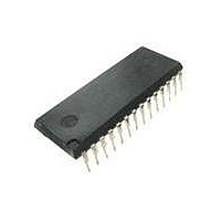
MC9S08RD32PE Freescale Semiconductor, MC9S08RD32PE Datasheet - Page 208

MC9S08RD32PE
Manufacturer Part Number
MC9S08RD32PE
Description
IC MCU 32K FLASH 2K RAM 28-DIP
Manufacturer
Freescale Semiconductor
Series
HCS08r
Datasheet
1.MC9S08RE8FJE.pdf
(234 pages)
Specifications of MC9S08RD32PE
Core Processor
HCS08
Core Size
8-Bit
Speed
8MHz
Connectivity
SCI
Peripherals
LVD, POR, PWM, WDT
Number Of I /o
23
Program Memory Size
32KB (32K x 8)
Program Memory Type
FLASH
Ram Size
2K x 8
Voltage - Supply (vcc/vdd)
1.8 V ~ 3.6 V
Oscillator Type
Internal
Operating Temperature
0°C ~ 70°C
Package / Case
28-DIP (0.600", 15.24mm)
Processor Series
S08RD
Core
HCS08
Data Bus Width
8 bit
Data Ram Size
2 KB
Interface Type
SCI
Maximum Clock Frequency
8 MHz
Number Of Programmable I/os
39
Number Of Timers
2
Operating Supply Voltage
1.8 V to 3.6 V
Maximum Operating Temperature
+ 70 C
Mounting Style
Through Hole
3rd Party Development Tools
EWS08
Development Tools By Supplier
DEMO9S08RG60E
Minimum Operating Temperature
0 C
Lead Free Status / RoHS Status
Lead free / RoHS Compliant
Eeprom Size
-
Data Converters
-
Lead Free Status / Rohs Status
Lead free / RoHS Compliant
Available stocks
Company
Part Number
Manufacturer
Quantity
Price
Company:
Part Number:
MC9S08RD32PE
Manufacturer:
Freescale Semiconductor
Quantity:
135
- Current page: 208 of 234
- Download datasheet (2Mb)
1. RAM will retain data down to POR voltage. RAM data not guaranteed to be valid following a POR.
2. This parameter is characterized and not tested on each device.
3. If SAFE bit is set, V
4. Measurement condition for pull resistors: V
5. The PTA0 pullup resistor may not pull up to the specified minimum V
6. All functional non-supply pins are internally clamped to V
Electrical Characteristics
208
Maximum low-voltage safe state re-arm
Input high voltage (V
Input high voltage (1.8 V ≤ V
Input low voltage (V
Input low voltage (1.8 V ≤ V
Input hysteresis (all digital inputs)
Input leakage current (Per pin)
High impedance (off-state) leakage current (per pin)
Internal pullup resistors
Internal pulldown resistor (IRQ)
Output high voltage (V
Output high voltage (port B and IRO)
Maximum total I
Output low voltage (V
Output low voltage (port B)
Output low voltage (IRO)
Maximum total I
dc injection current
Input capacitance (all non-supply pins)
Detect (LVD)
that a logic 1 will be read on any port input when the pullup is enabled and no dc load is present on the pin.
(all digital inputs)
I
I
I
I
I
I
I
Single pin limit
Total MCU limit, includes sum of all stressed pins
I
I
I
OH
OH
OH
OL
OL
OL
OL
V
V
I
OL
OL
OL
OH
In
In
= 2.0 mA (ports A, C, D and E)
= 6 mA (V
= 3 mA (V
= 16 mA (V
V
= –10 mA (V
= –6 mA (V
= –3 mA (V
= 10.0 mA (V
= 6 mA (V
= 3 mA (V
= V
= V
= –2 mA (ports A, C, D and E)
IN
< V
DD
DD
Table A-5. DC Characteristics (Temperature Range = –40 to 85°C Ambient) (continued)
or V
SS
or V
System.”
, V
OH
OL
DD
DD
DD
DD
SS
SS,
DD
DD
DD
IN
for all port pins
DD
for all port pins
≥ 2.3 V)
≥ 1.8 V)
(2), (6), (7), (8),, (9)
DD
DD
, all input/output
≥ 2.3 V)
≥ 1.8 V)
DD
DD
≥ 2.7 V)
> V
all input only pins
≥ 2.3 V)
≥ 1.8 V)
DD
≥ 2.7 V)
DD
≥ 2.7 V)
> 2.3 V) (all digital inputs)
(4) (5)
must be above re-arm voltage to allow MCU to accept interrupts, refer to
> 2.3 V) (all digital inputs)
DD
Parameter
≥ 1.8 V)
≥ 1.8 V)
DD
DD
≤ 2.3 V)
≤ 2.3 V) (all digital inputs)
MC9S08RC/RD/RE/RG Data Sheet, Rev. 1.11
(3)
In
= V
SS
for pullup and V
SS
and V
Symbol
V
|I
REARM
V
|I
R
R
V
I
V
DD
|I
V
V
|I
OHT
C
V
V
OLT
OZ
hys
OH
OL
IC
In
PU
PD
In
IH
IH
IL
IL
In
IH
.
|
|
|
= V
. However, all ports are functionally tested to guarantee
|
DD
0.70 × V
0.85 × V
0.06 × V
for pulldown.
V
V
DD
DD
17.5
17.5
Min
—
—
—
—
—
—
—
—
—
—
—
—
—
—
—
—
—
– 0.5
– 0.5
DD
DD
DD
Typical
0.025
0.025
—
Section 5.6, “Low-Voltage
Freescale Semiconductor
0.35 ×
0.30 ×
Max
52.5
52.5
V
V
3.0
1.0
1.0
0.5
0.5
0.5
0.5
1.2
1.2
1.2
0.2
60
60
—
—
—
—
—
—
—
5
7
DD
DD
Unit
κW
κW
mA
mA
mA
mA
µA
µA
pF
V
V
V
V
V
V
V
V
Related parts for MC9S08RD32PE
Image
Part Number
Description
Manufacturer
Datasheet
Request
R
Part Number:
Description:
Manufacturer:
Freescale Semiconductor, Inc
Datasheet:
Part Number:
Description:
Manufacturer:
Freescale Semiconductor, Inc
Datasheet:
Part Number:
Description:
Manufacturer:
Freescale Semiconductor, Inc
Datasheet:
Part Number:
Description:
Manufacturer:
Freescale Semiconductor, Inc
Datasheet:
Part Number:
Description:
Manufacturer:
Freescale Semiconductor, Inc
Datasheet:
Part Number:
Description:
Manufacturer:
Freescale Semiconductor, Inc
Datasheet:
Part Number:
Description:
Manufacturer:
Freescale Semiconductor, Inc
Datasheet:
Part Number:
Description:
Manufacturer:
Freescale Semiconductor, Inc
Datasheet:
Part Number:
Description:
Manufacturer:
Freescale Semiconductor, Inc
Datasheet:
Part Number:
Description:
Manufacturer:
Freescale Semiconductor, Inc
Datasheet:
Part Number:
Description:
Manufacturer:
Freescale Semiconductor, Inc
Datasheet:
Part Number:
Description:
Manufacturer:
Freescale Semiconductor, Inc
Datasheet:
Part Number:
Description:
Manufacturer:
Freescale Semiconductor, Inc
Datasheet:
Part Number:
Description:
Manufacturer:
Freescale Semiconductor, Inc
Datasheet:
Part Number:
Description:
Manufacturer:
Freescale Semiconductor, Inc
Datasheet:


