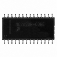
MC908GR4CDWE Freescale Semiconductor, MC908GR4CDWE Datasheet - Page 202

MC908GR4CDWE
Manufacturer Part Number
MC908GR4CDWE
Description
IC MCU 4K FLASH 8MHZ 28-SOIC
Manufacturer
Freescale Semiconductor
Series
HC08r
Specifications of MC908GR4CDWE
Core Processor
HC08
Core Size
8-Bit
Speed
8MHz
Connectivity
SCI, SPI
Peripherals
LVD, POR, PWM
Number Of I /o
17
Program Memory Size
4KB (4K x 8)
Program Memory Type
FLASH
Ram Size
384 x 8
Voltage - Supply (vcc/vdd)
2.7 V ~ 5.5 V
Data Converters
A/D 6x8b
Oscillator Type
Internal
Operating Temperature
-40°C ~ 85°C
Package / Case
28-SOIC (7.5mm Width)
Controller Family/series
HC08
No. Of I/o's
21
Ram Memory Size
384Byte
Cpu Speed
8MHz
No. Of Timers
1
Embedded Interface Type
I2C, SCI, SPI
Rohs Compliant
Yes
Processor Series
HC08GR
Core
HC08
Data Bus Width
8 bit
Data Ram Size
384 B
Interface Type
SCI, SPI
Maximum Clock Frequency
8.2 MHz
Number Of Programmable I/os
21
Number Of Timers
3
Maximum Operating Temperature
+ 85 C
Mounting Style
SMD/SMT
Development Tools By Supplier
FSICEBASE, DEMO908GZ60E, M68CBL05CE, M68EML08GPGTE
Minimum Operating Temperature
- 40 C
On-chip Adc
8 bit, 6 Channel
Lead Free Status / RoHS Status
Lead free / RoHS Compliant
Eeprom Size
-
Lead Free Status / Rohs Status
Details
- Current page: 202 of 408
- Download datasheet (4Mb)
Monitor ROM (MON)
15.5 Security
Technical Data
202
NOTE:
The MCU executes the SWI and PSHH instructions when it enters
monitor mode. The RUN command tells the MCU to execute the PULH
and RTI instructions. Before sending the RUN command, the host can
modify the stacked CPU registers to prepare to run the host program.
The READSP command returns the incremented stack pointer value,
SP + 1. The high and low bytes of the program counter are at addresses
SP + 5 and SP + 6.
A security feature discourages unauthorized reading of FLASH locations
while in monitor mode. The host can bypass the security feature at
monitor mode entry by sending eight security bytes that match the bytes
at locations $FFF6–$FFFD. Locations $FFF6–$FFFD contain user-
defined data.
Do not leave locations $FFF6–$FFFD blank. For security reasons, they
should be programmed even if they are not used for vectors.
During monitor mode entry, the MCU waits after the power-on reset for
the host to send the eight security bytes on pin PTA0. If the received
bytes match those at locations $FFF6–$FFFD, the host bypasses the
security feature and can read all FLASH locations and execute code
from FLASH. Security remains bypassed until a power-on reset occurs.
If the reset was not a power-on reset, security remains bypassed and
security code entry is not required. (See
Freescale Semiconductor, Inc.
For More Information On This Product,
Figure 15-7. Stack Pointer at Monitor Mode Entry
Go to: www.freescale.com
Monitor ROM (MON)
HIGH BYTE OF PROGRAM COUNTER
LOW BYTE OF PROGRAM COUNTER
HIGH BYTE OF INDEX REGISTER
LOW BYTE OF INDEX REGISTER
CONDITION CODE REGISTER
ACCUMULATOR
Figure
MC68HC908GR8 — Rev 4.0
SP + 1
SP + 2
SP + 3
SP + 4
SP + 5
15-8.)
SP
SP + 6
SP + 7
MOTOROLA
Related parts for MC908GR4CDWE
Image
Part Number
Description
Manufacturer
Datasheet
Request
R
Part Number:
Description:
Manufacturer:
Freescale Semiconductor, Inc
Datasheet:
Part Number:
Description:
Manufacturer:
Freescale Semiconductor, Inc
Datasheet:
Part Number:
Description:
Manufacturer:
Freescale Semiconductor, Inc
Datasheet:
Part Number:
Description:
Manufacturer:
Freescale Semiconductor, Inc
Datasheet:
Part Number:
Description:
Manufacturer:
Freescale Semiconductor, Inc
Datasheet:
Part Number:
Description:
Manufacturer:
Freescale Semiconductor, Inc
Datasheet:
Part Number:
Description:
Manufacturer:
Freescale Semiconductor, Inc
Datasheet:
Part Number:
Description:
Manufacturer:
Freescale Semiconductor, Inc
Datasheet:
Part Number:
Description:
Manufacturer:
Freescale Semiconductor, Inc
Datasheet:
Part Number:
Description:
Manufacturer:
Freescale Semiconductor, Inc
Datasheet:
Part Number:
Description:
Manufacturer:
Freescale Semiconductor, Inc
Datasheet:
Part Number:
Description:
Manufacturer:
Freescale Semiconductor, Inc
Datasheet:
Part Number:
Description:
Manufacturer:
Freescale Semiconductor, Inc
Datasheet:
Part Number:
Description:
Manufacturer:
Freescale Semiconductor, Inc
Datasheet:
Part Number:
Description:
Manufacturer:
Freescale Semiconductor, Inc
Datasheet:


