MC908GR4CDWE Freescale Semiconductor, MC908GR4CDWE Datasheet - Page 262
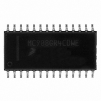
MC908GR4CDWE
Manufacturer Part Number
MC908GR4CDWE
Description
IC MCU 4K FLASH 8MHZ 28-SOIC
Manufacturer
Freescale Semiconductor
Series
HC08r
Specifications of MC908GR4CDWE
Core Processor
HC08
Core Size
8-Bit
Speed
8MHz
Connectivity
SCI, SPI
Peripherals
LVD, POR, PWM
Number Of I /o
17
Program Memory Size
4KB (4K x 8)
Program Memory Type
FLASH
Ram Size
384 x 8
Voltage - Supply (vcc/vdd)
2.7 V ~ 5.5 V
Data Converters
A/D 6x8b
Oscillator Type
Internal
Operating Temperature
-40°C ~ 85°C
Package / Case
28-SOIC (7.5mm Width)
Controller Family/series
HC08
No. Of I/o's
21
Ram Memory Size
384Byte
Cpu Speed
8MHz
No. Of Timers
1
Embedded Interface Type
I2C, SCI, SPI
Rohs Compliant
Yes
Processor Series
HC08GR
Core
HC08
Data Bus Width
8 bit
Data Ram Size
384 B
Interface Type
SCI, SPI
Maximum Clock Frequency
8.2 MHz
Number Of Programmable I/os
21
Number Of Timers
3
Maximum Operating Temperature
+ 85 C
Mounting Style
SMD/SMT
Development Tools By Supplier
FSICEBASE, DEMO908GZ60E, M68CBL05CE, M68EML08GPGTE
Minimum Operating Temperature
- 40 C
On-chip Adc
8 bit, 6 Channel
Lead Free Status / RoHS Status
Lead free / RoHS Compliant
Eeprom Size
-
Lead Free Status / Rohs Status
Details


Serial Communications Interface (SCI)
Technical Data
262
OR — Receiver Overrun Bit
NF — Receiver Noise Flag Bit
FE — Receiver Framing Error Bit
Freescale Semiconductor, Inc.
This clearable, read-only bit is set when software fails to read the
SCDR before the receive shift register receives the next character.
The OR bit generates an SCI error CPU interrupt request if the ORIE
bit in SCC3 is also set. The data in the shift register is lost, but the data
already in the SCDR is not affected. Clear the OR bit by reading SCS1
with OR set and then reading the SCDR. Reset clears the OR bit.
Software latency may allow an overrun to occur between reads of
SCS1 and SCDR in the flag-clearing sequence.
the normal flag-clearing sequence and an example of an overrun
caused by a delayed flag-clearing sequence. The delayed read of
SCDR does not clear the OR bit because OR was not set when SCS1
was read. Byte 2 caused the overrun and is lost. The next flag-
clearing sequence reads byte 3 in the SCDR instead of byte 2.
In applications that are subject to software latency or in which it is
important to know which byte is lost due to an overrun, the flag-
clearing routine can check the OR bit in a second read of SCS1 after
reading the data register.
This clearable, read-only bit is set when the SCI detects noise on the
PE1/RxD pin. NF generates an NF CPU interrupt request if the NEIE
bit in SCC3 is also set. Clear the NF bit by reading SCS1 and then
reading the SCDR. Reset clears the NF bit.
This clearable, read-only bit is set when a logic 0 is accepted as the
stop bit. FE generates an SCI error CPU interrupt request if the FEIE
bit in SCC3 also is set. Clear the FE bit by reading SCS1 with FE set
and then reading the SCDR. Reset clears the FE bit.
For More Information On This Product,
1 = Receive shift register full and SCRF = 1
0 = No receiver overrun
1 = Noise detected
0 = No noise detected
1 = Framing error detected
0 = No framing error detected
Serial Communications Interface (SCI)
Go to: www.freescale.com
MC68HC908GR8 — Rev 4.0
Figure 18-13
MOTOROLA
shows
Related parts for MC908GR4CDWE
Image
Part Number
Description
Manufacturer
Datasheet
Request
R

Part Number:
Description:
Manufacturer:
Freescale Semiconductor, Inc
Datasheet:
Part Number:
Description:
Manufacturer:
Freescale Semiconductor, Inc
Datasheet:
Part Number:
Description:
Manufacturer:
Freescale Semiconductor, Inc
Datasheet:
Part Number:
Description:
Manufacturer:
Freescale Semiconductor, Inc
Datasheet:
Part Number:
Description:
Manufacturer:
Freescale Semiconductor, Inc
Datasheet:
Part Number:
Description:
Manufacturer:
Freescale Semiconductor, Inc
Datasheet:
Part Number:
Description:
Manufacturer:
Freescale Semiconductor, Inc
Datasheet:
Part Number:
Description:
Manufacturer:
Freescale Semiconductor, Inc
Datasheet:
Part Number:
Description:
Manufacturer:
Freescale Semiconductor, Inc
Datasheet:
Part Number:
Description:
Manufacturer:
Freescale Semiconductor, Inc
Datasheet:
Part Number:
Description:
Manufacturer:
Freescale Semiconductor, Inc
Datasheet:
Part Number:
Description:
Manufacturer:
Freescale Semiconductor, Inc
Datasheet:
Part Number:
Description:
Manufacturer:
Freescale Semiconductor, Inc
Datasheet:
Part Number:
Description:
Manufacturer:
Freescale Semiconductor, Inc
Datasheet:
Part Number:
Description:
Manufacturer:
Freescale Semiconductor, Inc
Datasheet: