MC908AP32ACFBER Freescale Semiconductor, MC908AP32ACFBER Datasheet - Page 252
MC908AP32ACFBER
Manufacturer Part Number
MC908AP32ACFBER
Description
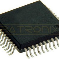
IC MCU 32K FLASH 8MHZ 44-QFP
Manufacturer
Freescale Semiconductor
Series
HC08r
Datasheet
1.MC908AP16ACFBER.pdf
(316 pages)
Specifications of MC908AP32ACFBER
Core Processor
HC08
Core Size
8-Bit
Speed
8MHz
Connectivity
I²C, IRSCI, SCI, SPI
Peripherals
LED, LVD, POR, PWM
Number Of I /o
32
Program Memory Size
32KB (32K x 8)
Program Memory Type
FLASH
Ram Size
2K x 8
Voltage - Supply (vcc/vdd)
4.5 V ~ 5.5 V
Data Converters
A/D 8x10b
Oscillator Type
Internal
Operating Temperature
-40°C ~ 85°C
Package / Case
44-QFP
Processor Series
HC08AP
Core
HC08
Data Bus Width
8 bit
Data Ram Size
2 KB
Interface Type
SCI, SPI
Maximum Clock Frequency
8 MHz
Number Of Programmable I/os
32
Number Of Timers
4
Maximum Operating Temperature
+ 85 C
Mounting Style
SMD/SMT
Development Tools By Supplier
FSICEBASE, DEMO908AP64E, M68CBL05CE
Minimum Operating Temperature
- 40 C
On-chip Adc
10 bit, 8 Channel
Lead Free Status / RoHS Status
Lead free / RoHS Compliant
Eeprom Size
-
Lead Free Status / Rohs Status
Details
Available stocks
Company
Part Number
Manufacturer
Quantity
Price
Company:

Part Number:
MC908AP32ACFBER
Manufacturer:
Freescale Semiconductor
Quantity:
10 000


Analog-to-Digital Converter (ADC)
15.7.2 ADC Clock Control Register
The ADC clock control register (ADICLK) selects the clock frequency for the ADC.
ADIV[2:0] — ADC Clock Prescaler Bits
252
ADCH4
NOTES:
1. If any unused channels are selected, the resulting ADC conversion will be unknown.
2. The voltage levels supplied from internal reference nodes as specified in the table are used to verify the operation of
ADIV2, ADIV1, and ADIV0 form a 3-bit field which selects the divide ratio used by the ADC to generate
the internal ADC clock.
Table 15-2
and 1MHz.
the ADC converter both in production test and for user applications.
0
0
0
0
0
0
0
0
0
↓
1
1
1
1
Address:
shows the available clock configurations. The ADC clock should be set to between 500kHz
ADCH3
signal. Recovery from the disabled state requires one conversion cycle to
stabilize.
Reset:
Read:
Write:
0
0
0
0
0
0
0
0
1
↓
1
1
1
1
ADIV2
$0058
0
Figure 15-4. ADC Clock Control Register (ADICLK)
ADCH2
0
0
0
0
1
1
1
1
0
↓
1
1
1
1
= Unimplemented
ADIV1
MC68HC908AP A-Family Data Sheet, Rev. 3
0
Table 15-1. MUX Channel Select
ADCH1
ADIV0
0
0
1
1
0
↓
0
0
0
1
1
0
1
1
0
ADICLK
ADCH0
0
↓
0
1
0
1
0
1
0
1
0
0
1
0
1
MODE1
R
0
ADC powered-off
ADC Channel
ADC28
ADC29
ADC30
ADC0
ADC1
ADC2
ADC3
ADC4
ADC5
ADC6
ADC7
ADC8
= Reserved
MODE0
↓
1
0
0
Freescale Semiconductor
V
V
REFH
REFL
Input Select
Reserved
R
0
0
(see Note 2)
(see Note 2)
PTA0
PTA1
PTA2
PTA3
PTA4
PTA5
PTA6
PTA7
—
Related parts for MC908AP32ACFBER
Image
Part Number
Description
Manufacturer
Datasheet
Request
R

Part Number:
Description:
Manufacturer:
Freescale Semiconductor, Inc
Datasheet:
Part Number:
Description:
Manufacturer:
Freescale Semiconductor, Inc
Datasheet:
Part Number:
Description:
Manufacturer:
Freescale Semiconductor, Inc
Datasheet:
Part Number:
Description:
Manufacturer:
Freescale Semiconductor, Inc
Datasheet:
Part Number:
Description:
Manufacturer:
Freescale Semiconductor, Inc
Datasheet:
Part Number:
Description:
Manufacturer:
Freescale Semiconductor, Inc
Datasheet:
Part Number:
Description:
Manufacturer:
Freescale Semiconductor, Inc
Datasheet:
Part Number:
Description:
Manufacturer:
Freescale Semiconductor, Inc
Datasheet:
Part Number:
Description:
Manufacturer:
Freescale Semiconductor, Inc
Datasheet:
Part Number:
Description:
Manufacturer:
Freescale Semiconductor, Inc
Datasheet:
Part Number:
Description:
Manufacturer:
Freescale Semiconductor, Inc
Datasheet:
Part Number:
Description:
Manufacturer:
Freescale Semiconductor, Inc
Datasheet:
Part Number:
Description:
Manufacturer:
Freescale Semiconductor, Inc
Datasheet:
Part Number:
Description:
Manufacturer:
Freescale Semiconductor, Inc
Datasheet:
Part Number:
Description:
Manufacturer:
Freescale Semiconductor, Inc
Datasheet: