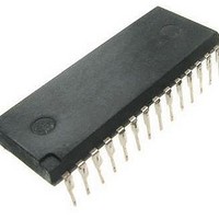
MC705P6ECPE Freescale Semiconductor, MC705P6ECPE Datasheet - Page 63

MC705P6ECPE
Manufacturer Part Number
MC705P6ECPE
Description
IC MCU 8BIT EPROM 28-DIP
Manufacturer
Freescale Semiconductor
Series
HC05r
Datasheet
1.MC705P6ACDWE.pdf
(98 pages)
Specifications of MC705P6ECPE
Core Processor
HC05
Core Size
8-Bit
Speed
2.1MHz
Connectivity
SIO
Peripherals
POR, WDT
Number Of I /o
21
Program Memory Size
4.5KB (4.5K x 8)
Program Memory Type
OTP
Ram Size
176 x 8
Voltage - Supply (vcc/vdd)
3 V ~ 5.5 V
Data Converters
A/D 4x8b
Oscillator Type
Internal
Operating Temperature
-40°C ~ 85°C
Package / Case
28-DIP (0.600", 15.24mm)
Processor Series
HC705P
Core
HC05
Data Bus Width
8 bit
Data Ram Size
176 B
Interface Type
SIOP
Maximum Clock Frequency
4.2 MHz
Number Of Programmable I/os
21
Number Of Timers
1
Operating Supply Voltage
- 0.3 V to + 7 V
Maximum Operating Temperature
+ 85 C
Mounting Style
Through Hole
Minimum Operating Temperature
- 40 C
On-chip Adc
8 bit, 4 Channel
On-chip Dac
8 bit, 4 Channel
Lead Free Status / RoHS Status
Lead free / RoHS Compliant
Eeprom Size
-
Lead Free Status / Rohs Status
Details
Available stocks
Company
Part Number
Manufacturer
Quantity
Price
Company:
Part Number:
MC705P6ECPE
Manufacturer:
Freescale Semiconductor
Quantity:
135
Chapter 11
Mask Option Register (MOR)
11.1 Introduction
The mask option register (MOR) contains two bytes of EPROM used to enable or disable each of the
features controlled by mask options on the MC68HC05P6 (a ROM version of the MC68HC705P6A).
The seven programmable options on the MC68HC705P6A are:
11.2 Mask Option Register
Mask options are programmed into the mask option register (MOR) by the firmware in the bootloader
ROM. See
COP — COP Watchdog Enable
Freescale Semiconductor
1. COP watchdog timer (enable or disable)
2. IRQ triggering (edge- or edge- and level-sensitive)
3. SIOP data bit order (most significant bit or least significant bit first)
4. SIOP clock rate (OSC divided by 8, 16, 32, or 64)
5. Stop instruction mode (stop mode or halt mode)
6. Secure EPROM from external reading
7. Keyscan interrupt/pullups on PA0–PA7
Setting the COP bit will enable the COP watchdog timer. The COP will reset the MCU if the timeout
period is reached before the COP watchdog timer is cleared by the application software and the
voltage applied to the IRQ/V
watchdog timer regardless of the voltage applied to the IRQ/V
Figure
Erased State:
Erased State:
Address: $1EFF
Address: $1F00
Read:
Read:
Write:
Write:
11-1.
SECURE
PA7PU
Bit 7
Bit 7
0
0
MC68HC705P6A Advance Information Data Sheet, Rev. 2.1
Figure 11-1. Mask Option Register (MOR)
PP
= Unimplemented
PA6PU
pin is between V
6
0
6
0
PA5PU
SWAIT
5
0
5
0
SS
PA4PU
SPR1
and V
4
0
4
0
DD
PA3PU
SPR0
. Clearing the COP bit will disable the COP
3
0
3
0
PP
pin.
PA2PU
LSBF
2
0
2
0
PA1PU
LEVEL
1
1
0
0
PA0PU
COP
Bit 0
Bit 0
0
0
63


