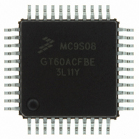
MC9S08GT60ACFDE Freescale Semiconductor, MC9S08GT60ACFDE Datasheet - Page 283

MC9S08GT60ACFDE
Manufacturer Part Number
MC9S08GT60ACFDE
Description
IC MCU 60K FLASH 4K RAM 48-QFN
Manufacturer
Freescale Semiconductor
Series
HCS08r
Datasheet
1.MC9S08GT60ACFDER.pdf
(302 pages)
Specifications of MC9S08GT60ACFDE
Core Processor
HCS08
Core Size
8-Bit
Speed
40MHz
Connectivity
I²C, SCI, SPI
Peripherals
LVD, POR, PWM, WDT
Number Of I /o
39
Program Memory Size
60KB (60K x 8)
Program Memory Type
FLASH
Ram Size
4K x 8
Voltage - Supply (vcc/vdd)
1.8 V ~ 3.6 V
Data Converters
A/D 8x10b
Oscillator Type
Internal
Operating Temperature
-40°C ~ 85°C
Package / Case
48-QFN
Processor Series
S08GT
Core
HCS08
Data Bus Width
8 bit
Data Ram Size
4 KB
Interface Type
SCI/SPI
Maximum Clock Frequency
40 MHz
Number Of Programmable I/os
39
Number Of Timers
2
Operating Supply Voltage
0 V to 1.8 V
Maximum Operating Temperature
+ 85 C
Mounting Style
SMD/SMT
3rd Party Development Tools
EWS08
Development Tools By Supplier
M68EVB908GB60E, M68DEMO908GB60E
Minimum Operating Temperature
- 40 C
On-chip Adc
8-ch x 10-bit
For Use With
M68DEMO908GB60E - BOARD DEMO MC9S08GB60M68EVB908GB60E - BOARD EVAL FOR MC9S08GB60
Lead Free Status / RoHS Status
Lead free / RoHS Compliant
Eeprom Size
-
Lead Free Status / Rohs Status
Lead free / RoHS Compliant
Available stocks
Company
Part Number
Manufacturer
Quantity
Price
- Current page: 283 of 302
- Download datasheet (8Mb)
Appendix B
EB652: Migrating from the GB60 Series to the GB60A Series
The following text was taken from Freescale Semiconductor document EB652. It is copied here for your
conveninece. Please see EB652 at freescale.com for the must up-to-date information regarding “Migrating
from the GB60 series to the GB60A series.”
B.1
This document will explain the differences to be aware of when migrating from the MC9S08GB60,
MC9S08GB32, MC9S08GT60, and MC9S08GT32 devices to the MC9S08GB60A, MC9S08GB32A,
MC9S08GT60A and MC9S08GT32A devices. For the remainder of this document, GB60 series will refer
to the original non-”A” devices and GB60A series will refer to the newer “A” suffix devices.
Much of the functionality and performance of the GB60 series and the GB60A series will be identical.
However, there are several differences designers should understand when migrating to the GB60A series.
B.2
The GB60 series has a minimum V
The GB60A series eliminates this minimum V
programmed and erased across the full operating voltage range of the MCU, or 1.8 V to 3.6 V.
B.3
The GB/GT60 flash block protection has a redundant setting. On the GB/GT60A, the redundant setting is
used to add a new protection option.
On the GB/GT60, when protection is enabled by setting the FPDIS bit, setting the FPS2:FPS1:FPS0 bits
to 1:1:1 protects the same range as 1:1:0, which is locations $8000 to $FFFF.
On the GB/GT60A, setting the FPS2:FPS1:FPS0 bits to 1:1:0, protects the same range as on the GB/GT60.
However, setting the bits to 1:1:1 protects locations $182C to $FFFF, leaving locations $1080 to $17FF
open to reprogramming.
This new protection option is useful for protecting the main user program area while leaving a small
section of 1920 bytes available for data storage.
B.4
The GB60 series only has a low-power external oscillator, designed for the low current consumption. The
GB60A series has a second external oscillator option: a high gain external oscillator which provides
Freescale Semiconductor
Overview
Flash Programming Voltage
Flash Block Protection: 60K Devices Only
Internal Clock Generator: High Gain Oscillator Option
DD
MC9S08GB60A Data Sheet, Rev. 2
requirement for erasing and programming the flash, equal to 2.1 V.
DD
requirement. On the GB60A series, the flash can be
283
Related parts for MC9S08GT60ACFDE
Image
Part Number
Description
Manufacturer
Datasheet
Request
R
Part Number:
Description:
Manufacturer:
Freescale Semiconductor, Inc
Datasheet:
Part Number:
Description:
Manufacturer:
Freescale Semiconductor, Inc
Datasheet:
Part Number:
Description:
Manufacturer:
Freescale Semiconductor, Inc
Datasheet:
Part Number:
Description:
Manufacturer:
Freescale Semiconductor, Inc
Datasheet:
Part Number:
Description:
Manufacturer:
Freescale Semiconductor, Inc
Datasheet:
Part Number:
Description:
Manufacturer:
Freescale Semiconductor, Inc
Datasheet:
Part Number:
Description:
Manufacturer:
Freescale Semiconductor, Inc
Datasheet:
Part Number:
Description:
Manufacturer:
Freescale Semiconductor, Inc
Datasheet:
Part Number:
Description:
Manufacturer:
Freescale Semiconductor, Inc
Datasheet:
Part Number:
Description:
Manufacturer:
Freescale Semiconductor, Inc
Datasheet:
Part Number:
Description:
Manufacturer:
Freescale Semiconductor, Inc
Datasheet:
Part Number:
Description:
Manufacturer:
Freescale Semiconductor, Inc
Datasheet:
Part Number:
Description:
Manufacturer:
Freescale Semiconductor, Inc
Datasheet:
Part Number:
Description:
Manufacturer:
Freescale Semiconductor, Inc
Datasheet:
Part Number:
Description:
Manufacturer:
Freescale Semiconductor, Inc
Datasheet:


