C8051F067-GQ Silicon Laboratories Inc, C8051F067-GQ Datasheet - Page 3
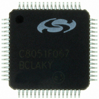
C8051F067-GQ
Manufacturer Part Number
C8051F067-GQ
Description
IC 8051 MCU 32K FLASH 64TQFP
Manufacturer
Silicon Laboratories Inc
Series
C8051F06xr
Specifications of C8051F067-GQ
Core Processor
8051
Core Size
8-Bit
Speed
25MHz
Connectivity
SMBus (2-Wire/I²C), SPI, UART/USART
Peripherals
Brown-out Detect/Reset, POR, PWM, WDT
Number Of I /o
24
Program Memory Size
32KB (32K x 8)
Program Memory Type
FLASH
Ram Size
4.25K x 8
Voltage - Supply (vcc/vdd)
2.7 V ~ 3.6 V
Data Converters
A/D 2x16b
Oscillator Type
Internal
Operating Temperature
-40°C ~ 85°C
Package / Case
64-TQFP, 64-VQFP
Processor Series
C8051F0x
Core
8051
Data Bus Width
8 bit
Data Ram Size
4.25 KB
Interface Type
I2C, SMBus, SPI, UART
Maximum Clock Frequency
25 MHz
Number Of Programmable I/os
24
Number Of Timers
5
Operating Supply Voltage
2.7 V to 3.6 V
Maximum Operating Temperature
+ 85 C
Mounting Style
SMD/SMT
3rd Party Development Tools
PK51, CA51, A51, ULINK2
Development Tools By Supplier
C8051F060DK
Minimum Operating Temperature
- 40 C
On-chip Adc
16 bit, 1 Channel
On-chip Dac
12 bit, 2 Channel
Lead Free Status / RoHS Status
Lead free / RoHS Compliant
Eeprom Size
-
Lead Free Status / Rohs Status
Details
Other names
336-1222
Available stocks
Company
Part Number
Manufacturer
Quantity
Price
Company:

Part Number:
C8051F067-GQ
Manufacturer:
AD
Quantity:
210
Company:
Part Number:
C8051F067-GQ
Manufacturer:
Silicon Laboratories Inc
Quantity:
10 000
Company:
Part Number:
C8051F067-GQR
Manufacturer:
Silicon Laboratories Inc
Quantity:
10 000


Table of Contents
1. System Overview.................................................................................................... 19
2. Absolute Maximum Ratings .................................................................................. 37
3. Global DC Electrical Characteristics .................................................................... 38
4. Pinout and Package Definitions............................................................................ 39
5. 16-Bit ADCs (ADC0 and ADC1) ............................................................................. 51
6. Direct Memory Access Interface (DMA0) ............................................................. 75
7. 10-Bit ADC (ADC2, C8051F060/1/2/3).................................................................... 87
1.1. CIP-51™ Microcontroller Core.......................................................................... 25
1.2. On-Chip Memory............................................................................................... 27
1.3. JTAG Debug and Boundary Scan..................................................................... 28
1.4. Programmable Digital I/O and Crossbar ........................................................... 29
1.5. Programmable Counter Array ........................................................................... 30
1.6. Controller Area Network.................................................................................... 31
1.7. Serial Ports ....................................................................................................... 32
1.8. 16-Bit Analog to Digital Converters................................................................... 33
1.9. 10-Bit Analog to Digital Converter..................................................................... 34
1.10.12-bit Digital to Analog Converters................................................................... 35
1.11.Analog Comparators......................................................................................... 36
5.1. Single-Ended or Differential Operation ............................................................. 52
5.2. Voltage Reference ............................................................................................ 53
5.3. ADC Modes of Operation.................................................................................. 54
5.4. Calibration......................................................................................................... 66
5.5. ADC0 Programmable Window Detector ........................................................... 69
6.1. Writing to the Instruction Buffer......................................................................... 75
6.2. DMA0 Instruction Format .................................................................................. 76
6.3. XRAM Addressing and Setup ........................................................................... 76
6.4. Instruction Execution in Mode 0........................................................................ 77
6.5. Instruction Execution in Mode 1........................................................................ 78
6.6. Interrupt Sources .............................................................................................. 79
6.7. Data Buffer Overflow Warnings and Errors....................................................... 79
7.1. Analog Multiplexer ............................................................................................ 88
7.2. Modes of Operation .......................................................................................... 89
1.1.1. Fully 8051 Compatible.............................................................................. 25
1.1.2. Improved Throughput ............................................................................... 25
1.1.3. Additional Features .................................................................................. 26
5.1.1. Pseudo-Differential Inputs ........................................................................ 52
5.3.1. Starting a Conversion............................................................................... 54
5.3.2. Tracking Modes........................................................................................ 54
5.3.3. Settling Time Requirements ..................................................................... 56
7.2.1. Starting a Conversion............................................................................... 89
7.2.2. Tracking Modes........................................................................................ 90
7.2.3. Settling Time Requirements ..................................................................... 91
Rev. 1.2
C8051F060/1/2/3/4/5/6/7
3
Related parts for C8051F067-GQ
Image
Part Number
Description
Manufacturer
Datasheet
Request
R

Part Number:
Description:
SMD/C°/SINGLE-ENDED OUTPUT SILICON OSCILLATOR
Manufacturer:
Silicon Laboratories Inc
Part Number:
Description:
Manufacturer:
Silicon Laboratories Inc
Datasheet:
Part Number:
Description:
N/A N/A/SI4010 AES KEYFOB DEMO WITH LCD RX
Manufacturer:
Silicon Laboratories Inc
Datasheet:
Part Number:
Description:
N/A N/A/SI4010 SIMPLIFIED KEY FOB DEMO WITH LED RX
Manufacturer:
Silicon Laboratories Inc
Datasheet:
Part Number:
Description:
N/A/-40 TO 85 OC/EZLINK MODULE; F930/4432 HIGH BAND (REV E/B1)
Manufacturer:
Silicon Laboratories Inc
Part Number:
Description:
EZLink Module; F930/4432 Low Band (rev e/B1)
Manufacturer:
Silicon Laboratories Inc
Part Number:
Description:
I°/4460 10 DBM RADIO TEST CARD 434 MHZ
Manufacturer:
Silicon Laboratories Inc
Part Number:
Description:
I°/4461 14 DBM RADIO TEST CARD 868 MHZ
Manufacturer:
Silicon Laboratories Inc
Part Number:
Description:
I°/4463 20 DBM RFSWITCH RADIO TEST CARD 460 MHZ
Manufacturer:
Silicon Laboratories Inc
Part Number:
Description:
I°/4463 20 DBM RADIO TEST CARD 868 MHZ
Manufacturer:
Silicon Laboratories Inc
Part Number:
Description:
I°/4463 27 DBM RADIO TEST CARD 868 MHZ
Manufacturer:
Silicon Laboratories Inc
Part Number:
Description:
I°/4463 SKYWORKS 30 DBM RADIO TEST CARD 915 MHZ
Manufacturer:
Silicon Laboratories Inc
Part Number:
Description:
N/A N/A/-40 TO 85 OC/4463 RFMD 30 DBM RADIO TEST CARD 915 MHZ
Manufacturer:
Silicon Laboratories Inc
Part Number:
Description:
I°/4463 20 DBM RADIO TEST CARD 169 MHZ
Manufacturer:
Silicon Laboratories Inc