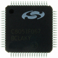
C8051F067-GQ Silicon Laboratories Inc, C8051F067-GQ Datasheet - Page 88

C8051F067-GQ
Manufacturer Part Number
C8051F067-GQ
Description
IC 8051 MCU 32K FLASH 64TQFP
Manufacturer
Silicon Laboratories Inc
Series
C8051F06xr
Specifications of C8051F067-GQ
Core Processor
8051
Core Size
8-Bit
Speed
25MHz
Connectivity
SMBus (2-Wire/I²C), SPI, UART/USART
Peripherals
Brown-out Detect/Reset, POR, PWM, WDT
Number Of I /o
24
Program Memory Size
32KB (32K x 8)
Program Memory Type
FLASH
Ram Size
4.25K x 8
Voltage - Supply (vcc/vdd)
2.7 V ~ 3.6 V
Data Converters
A/D 2x16b
Oscillator Type
Internal
Operating Temperature
-40°C ~ 85°C
Package / Case
64-TQFP, 64-VQFP
Processor Series
C8051F0x
Core
8051
Data Bus Width
8 bit
Data Ram Size
4.25 KB
Interface Type
I2C, SMBus, SPI, UART
Maximum Clock Frequency
25 MHz
Number Of Programmable I/os
24
Number Of Timers
5
Operating Supply Voltage
2.7 V to 3.6 V
Maximum Operating Temperature
+ 85 C
Mounting Style
SMD/SMT
3rd Party Development Tools
PK51, CA51, A51, ULINK2
Development Tools By Supplier
C8051F060DK
Minimum Operating Temperature
- 40 C
On-chip Adc
16 bit, 1 Channel
On-chip Dac
12 bit, 2 Channel
Lead Free Status / RoHS Status
Lead free / RoHS Compliant
Eeprom Size
-
Lead Free Status / Rohs Status
Details
Other names
336-1222
Available stocks
Company
Part Number
Manufacturer
Quantity
Price
Company:
Part Number:
C8051F067-GQ
Manufacturer:
AD
Quantity:
210
Company:
Part Number:
C8051F067-GQ
Manufacturer:
Silicon Laboratories Inc
Quantity:
10 000
Company:
Part Number:
C8051F067-GQR
Manufacturer:
Silicon Laboratories Inc
Quantity:
10 000
- Current page: 88 of 328
- Download datasheet (2Mb)
C8051F060/1/2/3/4/5/6/7
7.1.
The analog multiplexer (AMUX2) selects the inputs to the ADC, allowing any of the pins on Port 1 to be
measured in single-ended mode, or as a differential pair. Additionally, the on-chip temperature sensor may
be selected as a single-ended input. The ADC2 input channels are configured and selected in the
AMX2CF and AMX2SL registers as described in Figure 7.5 and Figure 7.6, respectively. In Single-ended
Mode, the selected pin is measured with respect to AGND. In Differential Mode, the selected differential
pair is measured with respect to one another. The polarity of the differential measurement depends on the
setting of the AMX2AD3-0 bits in the AMX2SL register. For example, if pins AIN2.0 and AIN2.1 are config-
ured for differential measurement (AIN01IC = 1), and AMX2AD3-0 = 0000b, the ADC will measure the volt-
age (AIN2.0 - AIN2.1). If AMX2AD3-0 is changed to 0001b, the ADC will measure the same voltage, with
opposite polarity (AIN2.1 - AIN2.0).
The conversion code format differs between Single-ended and Differential modes. The registers ADC2H
and ADC2L contain the high and low bytes of the output conversion code from the ADC at the completion
of each conversion. Data can be right-justified or left-justified, depending on the setting of the AD2LJST bit
(ADC2CN.0). When in Single-ended Mode, conversion codes are represented as 10-bit unsigned integers.
Inputs are measured from ‘0’ to VREF * 1023/1024. Example codes are shown below for both right-justified
and left-justified data. Unused bits in the ADC2H and ADC2L registers are set to ‘0’.
When in Differential Mode, conversion codes are represented as 10-bit signed 2’s complement numbers.
Inputs are measured from -VREF to VREF * 511/512. Example codes are shown below for both right-justi-
fied and left-justified data. For right-justified data, the unused MSBs of ADC2H are a sign-extension of the
data word. For left-justified data, the unused LSBs in the ADC2L register are set to ‘0’.
Important Note About ADC2 Input Configuration: Port 1 pins selected as ADC2 inputs should be con-
figured as analog inputs. To configure a Port 1 pin for analog input, set to ‘1’ the corresponding bit in regis-
ter P1MDIN. Port 1 pins used as ADC2 inputs will be skipped by the crossbar for peripheral assignments.
See
The Temperature Sensor transfer function is shown in Figure 7.2 on Page 89. The output voltage (V
is a single-ended input to ADC2 when the Temperature Sensor is selected by bits AMX2AD3-0 in register
AMX2SL. Typical values for the Slope and Offset parameters can be found in Table 7.1.
88
VREF * 1023/1024
VREF * 512/1024
VREF * 256/1024
-VREF * 256/512
VREF * 256/512
VREF * 511/512
Section “18. Port Input/Output” on page 203
Input Voltage
Input Voltage
Analog Multiplexer
- VREF
0
0
Right-Justified ADC2H:ADC2L
Right-Justified ADC2H:ADC2L
(AD2LJST = 0)
(AD2LJST = 0)
0xFE00
0x01FF
0xFF00
0x0100
0x0000
0x03FF
0x0200
0x0100
0x0000
for more Port I/O configuration details.
Rev. 1.2
Left-Justified ADC2H:ADC2L
Left-Justified ADC2H:ADC2L
(AD2LJST = 1)
(AD2LJST = 1)
0xFFC0
0x7FC0
0xC000
0x8000
0x4000
0x0000
0x4000
0x0000
0x8000
TEMP
)
Related parts for C8051F067-GQ
Image
Part Number
Description
Manufacturer
Datasheet
Request
R
Part Number:
Description:
SMD/C°/SINGLE-ENDED OUTPUT SILICON OSCILLATOR
Manufacturer:
Silicon Laboratories Inc
Part Number:
Description:
Manufacturer:
Silicon Laboratories Inc
Datasheet:
Part Number:
Description:
N/A N/A/SI4010 AES KEYFOB DEMO WITH LCD RX
Manufacturer:
Silicon Laboratories Inc
Datasheet:
Part Number:
Description:
N/A N/A/SI4010 SIMPLIFIED KEY FOB DEMO WITH LED RX
Manufacturer:
Silicon Laboratories Inc
Datasheet:
Part Number:
Description:
N/A/-40 TO 85 OC/EZLINK MODULE; F930/4432 HIGH BAND (REV E/B1)
Manufacturer:
Silicon Laboratories Inc
Part Number:
Description:
EZLink Module; F930/4432 Low Band (rev e/B1)
Manufacturer:
Silicon Laboratories Inc
Part Number:
Description:
I°/4460 10 DBM RADIO TEST CARD 434 MHZ
Manufacturer:
Silicon Laboratories Inc
Part Number:
Description:
I°/4461 14 DBM RADIO TEST CARD 868 MHZ
Manufacturer:
Silicon Laboratories Inc
Part Number:
Description:
I°/4463 20 DBM RFSWITCH RADIO TEST CARD 460 MHZ
Manufacturer:
Silicon Laboratories Inc
Part Number:
Description:
I°/4463 20 DBM RADIO TEST CARD 868 MHZ
Manufacturer:
Silicon Laboratories Inc
Part Number:
Description:
I°/4463 27 DBM RADIO TEST CARD 868 MHZ
Manufacturer:
Silicon Laboratories Inc
Part Number:
Description:
I°/4463 SKYWORKS 30 DBM RADIO TEST CARD 915 MHZ
Manufacturer:
Silicon Laboratories Inc
Part Number:
Description:
N/A N/A/-40 TO 85 OC/4463 RFMD 30 DBM RADIO TEST CARD 915 MHZ
Manufacturer:
Silicon Laboratories Inc
Part Number:
Description:
I°/4463 20 DBM RADIO TEST CARD 169 MHZ
Manufacturer:
Silicon Laboratories Inc


