M30281F6HP#U5B Renesas Electronics America, M30281F6HP#U5B Datasheet - Page 287
M30281F6HP#U5B
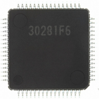
Manufacturer Part Number
M30281F6HP#U5B
Description
IC M16C/28 MCU FLASH 48K 64LQFP
Manufacturer
Renesas Electronics America
Series
M16C™ M16C/Tiny/28r
Datasheet
1.M30280F6HPU9.pdf
(425 pages)
Specifications of M30281F6HP#U5B
Core Processor
M16C/60
Core Size
16-Bit
Speed
20MHz
Connectivity
I²C, IEBus, SIO, UART/USART
Peripherals
DMA, POR, PWM, Voltage Detect, WDT
Number Of I /o
55
Program Memory Size
48KB (48K x 8)
Program Memory Type
FLASH
Ram Size
4K x 8
Voltage - Supply (vcc/vdd)
2.7 V ~ 5.5 V
Data Converters
A/D 13x10b
Oscillator Type
Internal
Operating Temperature
-20°C ~ 85°C
Package / Case
64-LQFP
For Use With
R0K330290S000BE - KIT EVAL STARTER FOR M16C/29M30290T2-CPE - EMULATOR COMPACT M16C/26A/28/29M30290T2-CPE-HP - EMULATOR COMPACT FOR M16C/TINY
Lead Free Status / RoHS Status
Lead free / RoHS Compliant
Eeprom Size
-
Available stocks
Company
Part Number
Manufacturer
Quantity
Price

Part Number:
M30281F6HP#U5BM30281F6HP#D5
Manufacturer:
Renesas Electronics America
Quantity:
10 000
Part Number:
M30281F6HP#U5BM30281F6HP#U3
Manufacturer:
Renesas Electronics America
Quantity:
10 000


R
R
M
e
E
1
Figure 16.11 Interrupt request signal generation timing
. v
J
6
0
16.5.5 Bit 4: I
16.5.6 Bit 5: Bus Busy Flag (BB)
C
2
9
The PIN bit generates an I
PIN bit is changed from “1” to “0”. At the same time, an I
The PIN bit is synchronized with the last clock of the internal transfer clock (when ACK-CLK=1, the last
clock is the ACK clock: when the ACK-CLK=0, the last clock is the 8th clock) and it becomes "0". The
interrupt request is generated on the falling edge of the PIN bit. When the PIN bit is set to "0", the clock
applied to SCL maintains "L" and further clock generation is disabled. When the ACK-CLK bit is set to "1"
and the WIT bit in the S3D0 register is set to "1" (enable the I
completion). The PIN bit is synchronized with the last clock and the falling edge of the ACK clock. Then,
the PIN bit is set to "0" and I
timing of the I
The BB flag indicates the operating conditions of the bus system. When the BB flag is set to “0”, a bus
system is not in use and a START condition can be generated. The BB flag is set and reset based on an
input signal of the SCL and SDA pins either in master mode or in slave mode. When the START condition
is detected, the BB flag is set to "1". On the other hand, when the STOP condition is detected, the BB flag
is set to "0". The SSC4 to SSC0 bits in the S2D0 register decide to detect between the START condition
and the STOP condition. When the ES0 bit in the S1D0 register is set to "0" (I
or when the IHR bit in the S1D0 register is set to "1" (reset), the BB flag is set to "0". Refer to 16.9 START
Condition Generation Method and 16.11 STOP Condition Generation Method.
0 .
2 /
B
The PIN bit is set to “1” in one of the following conditions:
The PIN bit is set to “0” in one of the following conditions:
0
0
8
0
•When data is written to the S00 register
•When data is written to the S20 register (when the WIT bit is set to “1” and the internal WAIT flag is
•When the ES0 bit in the S1D0 register is set to “0” (I
•When the IHR bit in the S1D0 register is set to "1"(reset)
•With completion of 1-byte data transmit (including a case when arbitration lost is detected)
•With completion of 1-byte data receive
•When the ALS bit in the S1D0 register is set to "0" (addressing format) and slave address is matched
•When the ALS bit is set to "1" (free format) and the address data is received successfully in slave
4
G
J
set to “1”)
or general call address is received successfully in slave receive mode
receive mode
7
a
o r
0 -
. n
u
2
3
p
0
, 1
0
(
M
2
0
1
2
0
C bus interface interrupt request generation.
6
7
2
C
C bus Interface Interrupt Request Bit (PIN)
2 /
page 265
, 8
M
1
PIN flag
I
6
2
2
CIRQ
C
C bus interface interrupt request signal. Every one byte data is ransferred, the
S
f o
2 /
CL
2
8
C bus interface interrupt request is generated. Figure 16.11 shows the
3
) B
8
5
2
2
C bus interface interrupt request is generated.
C bus interface disabled)
2
C bus interface interrupt of data receive
16. MULTI-MASTER I
2
C bus interface disabled)
2
C bus INTERFACE
Related parts for M30281F6HP#U5B
Image
Part Number
Description
Manufacturer
Datasheet
Request
R

Part Number:
Description:
KIT STARTER FOR M16C/29
Manufacturer:
Renesas Electronics America
Datasheet:

Part Number:
Description:
KIT STARTER FOR R8C/2D
Manufacturer:
Renesas Electronics America
Datasheet:

Part Number:
Description:
R0K33062P STARTER KIT
Manufacturer:
Renesas Electronics America
Datasheet:

Part Number:
Description:
KIT STARTER FOR R8C/23 E8A
Manufacturer:
Renesas Electronics America
Datasheet:

Part Number:
Description:
KIT STARTER FOR R8C/25
Manufacturer:
Renesas Electronics America
Datasheet:

Part Number:
Description:
KIT STARTER H8S2456 SHARPE DSPLY
Manufacturer:
Renesas Electronics America
Datasheet:

Part Number:
Description:
KIT STARTER FOR R8C38C
Manufacturer:
Renesas Electronics America
Datasheet:

Part Number:
Description:
KIT STARTER FOR R8C35C
Manufacturer:
Renesas Electronics America
Datasheet:

Part Number:
Description:
KIT STARTER FOR R8CL3AC+LCD APPS
Manufacturer:
Renesas Electronics America
Datasheet:
Part Number:
Description:
KIT STARTER FOR RX610
Manufacturer:
Renesas Electronics America
Datasheet:

Part Number:
Description:
KIT STARTER FOR R32C/118
Manufacturer:
Renesas Electronics America
Datasheet:

Part Number:
Description:
KIT DEV RSK-R8C/26-29
Manufacturer:
Renesas Electronics America
Datasheet:

Part Number:
Description:
KIT STARTER FOR SH7124
Manufacturer:
Renesas Electronics America
Datasheet:

Part Number:
Description:
KIT STARTER FOR H8SX/1622
Manufacturer:
Renesas Electronics America
Datasheet:

Part Number:
Description:
KIT DEV FOR SH7203
Manufacturer:
Renesas Electronics America
Datasheet: