MCF5212CAE66 Freescale Semiconductor, MCF5212CAE66 Datasheet - Page 10
MCF5212CAE66
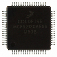
Manufacturer Part Number
MCF5212CAE66
Description
IC MCU 256K FLASH 66MHZ 64-LQFP
Manufacturer
Freescale Semiconductor
Series
MCF521xr
Datasheet
1.MCF5213CAF80.pdf
(54 pages)
Specifications of MCF5212CAE66
Core Processor
Coldfire V2
Core Size
32-Bit
Speed
66MHz
Connectivity
I²C, SPI, UART/USART
Peripherals
DMA, LVD, POR, PWM, WDT
Number Of I /o
55
Program Memory Size
256KB (256K x 8)
Program Memory Type
FLASH
Ram Size
32K x 8
Voltage - Supply (vcc/vdd)
3 V ~ 3.6 V
Data Converters
A/D 8x12b
Oscillator Type
Internal
Operating Temperature
-40°C ~ 85°C
Package / Case
64-LQFP
Processor Series
MCF521x
Core
ColdFire V2
Data Bus Width
32 bit
Data Ram Size
32 KB
Interface Type
I2C, QSPI, UART
Maximum Clock Frequency
80 MHz
Number Of Programmable I/os
56
Number Of Timers
10
Operating Supply Voltage
3 V to 3.6 V
Maximum Operating Temperature
+ 105 C
Mounting Style
SMD/SMT
3rd Party Development Tools
JLINK-CF-BDM26, EWCF
Development Tools By Supplier
M52210DEMO, M52211EVB
Minimum Operating Temperature
0 C
On-chip Adc
12 bit, 8 Channel
For Use With
M5211DEMO - KIT DEMO FOR MCF5211
Lead Free Status / RoHS Status
Lead free / RoHS Compliant
Eeprom Size
-
Lead Free Status / Rohs Status
Lead free / RoHS Compliant
Available stocks
Company
Part Number
Manufacturer
Quantity
Price
Company:

Part Number:
MCF5212CAE66
Manufacturer:
FREESCAL
Quantity:
1 210
Company:
Part Number:
MCF5212CAE66
Manufacturer:
Freescale Semiconductor
Quantity:
10 000
Part Number:
MCF5212CAE66
Manufacturer:
FREESCALE
Quantity:
20 000


Family Configurations
1.2.7
The FlexCAN module is a communication controller implementing version 2.0 of the CAN protocol parts A and B. The CAN
protocol can be used as an industrial control serial data bus, meeting the specific requirements of reliable operation in a harsh
EMI environment with high bandwidth. This instantiation of FlexCAN has 16 message buffers.
1.2.8
The device has three full-duplex UARTs that function independently. The three UARTs can be clocked by the system bus clock,
eliminating the need for an external clock source. On smaller packages, the third UART is multiplexed with other digital I/O
functions.
1.2.9
The I
and minimizes the interconnection between devices. This bus is suitable for applications requiring occasional communications
over a short distance between many devices.
1.2.10
The queued serial peripheral interface (QSPI) provides a synchronous serial peripheral interface with queued transfer capability.
It allows up to 16 transfers to be queued at once, minimizing the need for CPU intervention between transfers.
1.2.11
The fast ADC consists of an eight-channel input select multiplexer and two independent sample and hold (S/H) circuits feeding
separate 12-bit ADCs. The two separate converters store their results in accessible buffers for further processing.
The ADC can be configured to perform a single scan and halt, a scan when triggered, or a programmed scan sequence repeatedly
until manually stopped.
The ADC can be configured for sequential or simultaneous conversion. When configured for sequential conversions, up to eight
channels can be sampled and stored in any order specified by the channel list register. Both ADCs may be required during a
scan, depending on the inputs to be sampled.
During a simultaneous conversion, both S/H circuits are used to capture two different channels at the same time. This
configuration requires that a single channel may not be sampled by both S/H circuits simultaneously.
Optional interrupts can be generated at the end of the scan sequence if a channel is out of range (measures below the low
threshold limit or above the high threshold limit set in the limit registers) or at several different zero crossing conditions.
1.2.12
There are four independent, DMA transfer capable 32-bit timers (DTIM0, DTIM1, DTIM2, and DTIM3) on the device. Each
module incorporates a 32-bit timer with a separate register set for configuration and control. The timers can be configured to
operate from the system clock or from an external clock source using one of the DTINn signals. If the system clock is selected,
it can be divided by 16 or 1. The input clock is further divided by a user-programmable 8-bit prescaler that clocks the actual
timer counter register (TCRn). Each of these timers can be configured for input capture or reference (output) compare mode.
Timer events may optionally cause interrupt requests or DMA transfers.
10
2
C bus is an industry-standard, two-wire, bidirectional serial bus that provides a simple, efficient method of data exchange
FlexCAN
UARTs
I
QSPI
Fast ADC
DMA Timers (DTIM0–DTIM3)
2
C Bus
MCF5213 ColdFire Microcontroller, Rev. 4
Freescale Semiconductor
Related parts for MCF5212CAE66
Image
Part Number
Description
Manufacturer
Datasheet
Request
R

Part Number:
Description:
Microcontroller Family Hardware Specification
Manufacturer:
FREESCALE [Freescale Semiconductor, Inc]
Datasheet:

Part Number:
Description:
Manufacturer:
Freescale Semiconductor, Inc
Datasheet:
Part Number:
Description:
Manufacturer:
Freescale Semiconductor, Inc
Datasheet:
Part Number:
Description:
Manufacturer:
Freescale Semiconductor, Inc
Datasheet:
Part Number:
Description:
Manufacturer:
Freescale Semiconductor, Inc
Datasheet:
Part Number:
Description:
Manufacturer:
Freescale Semiconductor, Inc
Datasheet:
Part Number:
Description:
Manufacturer:
Freescale Semiconductor, Inc
Datasheet:
Part Number:
Description:
Manufacturer:
Freescale Semiconductor, Inc
Datasheet:
Part Number:
Description:
Manufacturer:
Freescale Semiconductor, Inc
Datasheet:
Part Number:
Description:
Manufacturer:
Freescale Semiconductor, Inc
Datasheet:
Part Number:
Description:
Manufacturer:
Freescale Semiconductor, Inc
Datasheet:
Part Number:
Description:
Manufacturer:
Freescale Semiconductor, Inc
Datasheet:
Part Number:
Description:
Manufacturer:
Freescale Semiconductor, Inc
Datasheet:
Part Number:
Description:
Manufacturer:
Freescale Semiconductor, Inc
Datasheet:
Part Number:
Description:
Manufacturer:
Freescale Semiconductor, Inc
Datasheet: