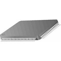
MC68HC11K1CFUE3 Freescale Semiconductor, MC68HC11K1CFUE3 Datasheet - Page 145

MC68HC11K1CFUE3
Manufacturer Part Number
MC68HC11K1CFUE3
Description
MCU 8-BIT 768 RAM 3MHZ 80-QFP
Manufacturer
Freescale Semiconductor
Series
HC11r
Specifications of MC68HC11K1CFUE3
Core Processor
HC11
Core Size
8-Bit
Speed
3MHz
Connectivity
SCI, SPI
Peripherals
POR, PWM, WDT
Number Of I /o
37
Program Memory Type
ROMless
Eeprom Size
640 x 8
Ram Size
768 x 8
Voltage - Supply (vcc/vdd)
4.5 V ~ 5.5 V
Data Converters
A/D 8x8b
Oscillator Type
Internal
Operating Temperature
-40°C ~ 85°C
Package / Case
80-QFP
Data Bus Width
8 bit
Data Ram Size
768 B
Interface Type
SCI, SPI
Maximum Clock Frequency
4 MHz
Number Of Programmable I/os
37
Number Of Timers
8
Maximum Operating Temperature
+ 85 C
Mounting Style
SMD/SMT
Minimum Operating Temperature
- 40 C
On-chip Adc
8 bit, 8 Channel
Lead Free Status / RoHS Status
Lead free / RoHS Compliant
Program Memory Size
-
Lead Free Status / Rohs Status
Details
Available stocks
Company
Part Number
Manufacturer
Quantity
Price
Company:
Part Number:
MC68HC11K1CFUE3
Manufacturer:
FREESCALE
Quantity:
8 831
Company:
Part Number:
MC68HC11K1CFUE3
Manufacturer:
Freescale Semiconductor
Quantity:
10 000
- Current page: 145 of 290
- Download datasheet (4Mb)
6.9 Port G
M68HC11K Family
MOTOROLA
Alternate Pin Function:
1. Not available on KS devices
1. Not available on KS devices
Address: $007E
Address: $007F
The state of port G pin 7 (PG7) at reset is mode dependent. In
single-chip or bootstrap modes, it is a high-impedance input; its data
direction can be changed through DDRG. In expanded and special test
modes, PG7 functions as the R/W line to control the direction of data flow
between the MCU and external memory devices.
Port G pins (PG[6:0]) reset to high-impedance inputs in any mode. Data
direction can be changed through DDRG. Port G bits [5:0] can serve as
memory expansion address lines (see
expanded and special test modes. M68HC11KS devices do not contain
these pins.
All eight port G pins have selectable internal pullup resistors (see
Internal Pullup
DDG[7:0] — Data Direction for Port G Bits
Reset:
Reset:
Read:
Read:
Write:
Write:
Freescale Semiconductor, Inc.
Figure 6-14. Port G Data Direction Register (DDRG)
For More Information On This Product,
0 = Input
1 = Output
Figure 6-13. Port G Data Register (PORTG)
DDG7
Bit 7
PG7
R/W
Bit 7
0
0
Go to: www.freescale.com
Parallel Input/Output
DDG6
PG6
Resistors).
—
6
0
6
0
(1)
(1)
DDG5
PG5
XA18
5
0
5
0
(1)
(1)
DDG4
PG4
XA17
4
0
4
0
(1)
(1)
11.3 Memory
DDG3
PG3
XA16
3
0
3
0
(1)
(1)
DDG2
PG2
XA15
2
0
2
0
(1)
(1)
Expansion) in
Parallel Input/Output
DDG1
PG1
XA14
1
0
1
0
Technical Data
(1)
(1)
DDG0
PG0
XA13
6.11
Bit 0
Bit 0
Port G
0
0
(1)
145
(1)
Related parts for MC68HC11K1CFUE3
Image
Part Number
Description
Manufacturer
Datasheet
Request
R

Part Number:
Description:
MC68HC11 EEPROM Programming from a Personal Computer
Manufacturer:
Motorola / Freescale Semiconductor
Part Number:
Description:
Manufacturer:
Freescale Semiconductor, Inc
Datasheet:
Part Number:
Description:
Manufacturer:
Freescale Semiconductor, Inc
Datasheet:
Part Number:
Description:
Manufacturer:
Freescale Semiconductor, Inc
Datasheet:
Part Number:
Description:
Manufacturer:
Freescale Semiconductor, Inc
Datasheet:
Part Number:
Description:
Manufacturer:
Freescale Semiconductor, Inc
Datasheet:
Part Number:
Description:
Manufacturer:
Freescale Semiconductor, Inc
Datasheet:
Part Number:
Description:
Manufacturer:
Freescale Semiconductor, Inc
Datasheet:
Part Number:
Description:
Manufacturer:
Freescale Semiconductor, Inc
Datasheet:
Part Number:
Description:
Manufacturer:
Freescale Semiconductor, Inc
Datasheet:
Part Number:
Description:
Manufacturer:
Freescale Semiconductor, Inc
Datasheet:
Part Number:
Description:
Manufacturer:
Freescale Semiconductor, Inc
Datasheet:
Part Number:
Description:
Manufacturer:
Freescale Semiconductor, Inc
Datasheet:
Part Number:
Description:
Manufacturer:
Freescale Semiconductor, Inc
Datasheet:
Part Number:
Description:
Manufacturer:
Freescale Semiconductor, Inc
Datasheet:


