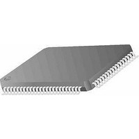
MC68HC11K1CFUE3 Freescale Semiconductor, MC68HC11K1CFUE3 Datasheet - Page 196

MC68HC11K1CFUE3
Manufacturer Part Number
MC68HC11K1CFUE3
Description
MCU 8-BIT 768 RAM 3MHZ 80-QFP
Manufacturer
Freescale Semiconductor
Series
HC11r
Specifications of MC68HC11K1CFUE3
Core Processor
HC11
Core Size
8-Bit
Speed
3MHz
Connectivity
SCI, SPI
Peripherals
POR, PWM, WDT
Number Of I /o
37
Program Memory Type
ROMless
Eeprom Size
640 x 8
Ram Size
768 x 8
Voltage - Supply (vcc/vdd)
4.5 V ~ 5.5 V
Data Converters
A/D 8x8b
Oscillator Type
Internal
Operating Temperature
-40°C ~ 85°C
Package / Case
80-QFP
Data Bus Width
8 bit
Data Ram Size
768 B
Interface Type
SCI, SPI
Maximum Clock Frequency
4 MHz
Number Of Programmable I/os
37
Number Of Timers
8
Maximum Operating Temperature
+ 85 C
Mounting Style
SMD/SMT
Minimum Operating Temperature
- 40 C
On-chip Adc
8 bit, 8 Channel
Lead Free Status / RoHS Status
Lead free / RoHS Compliant
Program Memory Size
-
Lead Free Status / Rohs Status
Details
Available stocks
Company
Part Number
Manufacturer
Quantity
Price
Company:
Part Number:
MC68HC11K1CFUE3
Manufacturer:
FREESCALE
Quantity:
8 831
Company:
Part Number:
MC68HC11K1CFUE3
Manufacturer:
Freescale Semiconductor
Quantity:
10 000
- Current page: 196 of 290
- Download datasheet (4Mb)
Timing System
9.6 Output Compare (OC)
Technical Data
196
The output compare (OC) function generates a programmed action
when the 16-bit counter reaches a specified value. Each of the five
output compare functions contains a separate 16-bit timer output
compare (TOC) register and a dedicated 16-bit comparator. Each TOC
register is set to $FFFF on reset. When an OC channel is enabled, the
value in its TOC register is compared to the free-running counter value
during each E-clock cycle. When the values match, the channel’s output
compare flag is set in timer interrupt flag 1 (TFLG1). If the channel’s
interrupt is enabled in the timer interrupt mask register 1 (TMSK1), an
interrupt is generated. Also, the corresponding timer output pin is
toggled or driven to a specified logic level. This pin activity occurs on
each successful compare, whether or not the OCxF flag in the TFLG1
register was previously cleared.
The pin action for each of the OC channels [5:2] is controlled by a pair of
bits (OMx and OLx) in the TCTL1 register and affects only the channel’s
associated pin. A successful OC1 compare can affect any or all five of
the OC pins. The action taken when a match is found for OC1 is
controlled by two 8-bit registers:
OC1M specifies which port A outputs are to be used, and OC1D
specifies the data placed on these port pins.
Although the M68HC11K series devices have four built-in pulse-width
modulation (PWM) channels
output compare function can be used to produce an additional
pulse-width modulated waveform. To produce a pulse of a specific
duration:
•
•
•
•
Freescale Semiconductor, Inc.
For More Information On This Product,
Output compare 1 mask register (OC1M)
Output compare 1 data register (OC1D)
Write a value to the output compare register that represents the
time the leading edge of the pulse is to occur.
Use OC1D to select either a high or low output, depending on the
polarity of the pulse being produced.
Go to: www.freescale.com
Timing System
(9.9 Pulse-Width Modulator
M68HC11K Family
(PWM)), the
MOTOROLA
Related parts for MC68HC11K1CFUE3
Image
Part Number
Description
Manufacturer
Datasheet
Request
R

Part Number:
Description:
MC68HC11 EEPROM Programming from a Personal Computer
Manufacturer:
Motorola / Freescale Semiconductor
Part Number:
Description:
Manufacturer:
Freescale Semiconductor, Inc
Datasheet:
Part Number:
Description:
Manufacturer:
Freescale Semiconductor, Inc
Datasheet:
Part Number:
Description:
Manufacturer:
Freescale Semiconductor, Inc
Datasheet:
Part Number:
Description:
Manufacturer:
Freescale Semiconductor, Inc
Datasheet:
Part Number:
Description:
Manufacturer:
Freescale Semiconductor, Inc
Datasheet:
Part Number:
Description:
Manufacturer:
Freescale Semiconductor, Inc
Datasheet:
Part Number:
Description:
Manufacturer:
Freescale Semiconductor, Inc
Datasheet:
Part Number:
Description:
Manufacturer:
Freescale Semiconductor, Inc
Datasheet:
Part Number:
Description:
Manufacturer:
Freescale Semiconductor, Inc
Datasheet:
Part Number:
Description:
Manufacturer:
Freescale Semiconductor, Inc
Datasheet:
Part Number:
Description:
Manufacturer:
Freescale Semiconductor, Inc
Datasheet:
Part Number:
Description:
Manufacturer:
Freescale Semiconductor, Inc
Datasheet:
Part Number:
Description:
Manufacturer:
Freescale Semiconductor, Inc
Datasheet:
Part Number:
Description:
Manufacturer:
Freescale Semiconductor, Inc
Datasheet:


