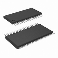
COP8CCE9IMT7/NOPB National Semiconductor, COP8CCE9IMT7/NOPB Datasheet - Page 18

COP8CCE9IMT7/NOPB
Manufacturer Part Number
COP8CCE9IMT7/NOPB
Description
MCU 8BIT FLASH 8K MEM 48-TSSOP
Manufacturer
National Semiconductor
Series
COP8™ 8Cr
Datasheet
1.I2C-CPEV.pdf
(80 pages)
Specifications of COP8CCE9IMT7/NOPB
Core Processor
COP8
Core Size
8-Bit
Speed
10MHz
Connectivity
Microwire/Plus (SPI), UART/USART
Peripherals
Brown-out Detect/Reset, POR, PWM, WDT
Number Of I /o
39
Program Memory Size
8KB (8K x 8)
Program Memory Type
FLASH
Ram Size
256 x 8
Voltage - Supply (vcc/vdd)
2.7 V ~ 5.5 V
Data Converters
A/D 16x10b
Oscillator Type
Internal
Operating Temperature
-40°C ~ 125°C
Package / Case
48-TSSOP
Data Bus Width
8 bit
Maximum Clock Frequency
10 MHz
Data Ram Size
256 B
On-chip Adc
10 bit, 16 channel
Number Of Programmable I/os
37
Number Of Timers
2
Height
0.9 mm
Interface Type
SPI, USART
Length
12.5 mm
Maximum Operating Temperature
+ 125 C
Minimum Operating Temperature
- 40 C
Supply Voltage (max)
5.5 V
Supply Voltage (min)
2.7 V
Width
6.1 mm
Lead Free Status / RoHS Status
Lead free / RoHS Compliant
Eeprom Size
-
Lead Free Status / Rohs Status
Details
Other names
COP8CCE9IMT7
www.national.com
9.0 Pin Descriptions
ration registers for G6 and G7 are used for special purpose
functions as outlined below. Reading the G6 and G7 data
bits will return zeros.
The device will be placed in the HALT mode by writing a “1”
to bit 7 of the Port G Data Register. Similarly the device will
be placed in the IDLE mode by writing a “1” to bit 6 of the
Port G Data Register.
Writing a “1” to bit 6 of the Port G Configuration Register
enables the MICROWIRE/PLUS to operate with the alter-
nate phase of the SK clock. The G7 configuration bit, if set
high, enables the clock start up delay after HALT when the
R/C clock configuration is used.
Port G has the following alternate features:
G7 CKO Oscillator dedicated output
G6 SI (MICROWIRE/PLUS Serial Data Input)
G5 SK (MICROWIRE/PLUS Serial Clock)
G4 SO (MICROWIRE/PLUS Serial Data Output)
G3 T1A (Timer T1 I/O)
G2 T1B (Timer T1 Capture Input)
G1 WDOUT WATCHDOG and/or Clock Monitor if WATCH-
G0 INTR (External Interrupt Input)
G0 through G3 are also used for In-System Emulation.
Port H is an 8-bit I/O port. All H pins have Schmitt triggers on
the inputs.
Port L is an 8-bit I/O port. All L-pins have Schmitt triggers on
the inputs.
Port L supports the Multi-Input Wake-up feature on all eight
pins. Port L has the following alternate pin functions:
L7 Multi-Input Wake-up
L6 Multi-Input Wake-up
L5 Multi-Input Wake-up or T2B (Timer T2B Input)
L4 Multi-input Wake-up or T2A (Timer T2A Input/Output)
L3 Multi-Input Wake-up and/or RDX (USART Receive)
L2 Multi-Input Wake-up or TDX (USART Transmit)
L1 Multi-Input Wake-up and/or CKX (USART Clock) (Low
L0 Multi-Input Wake-up (Low Speed Oscillator Input)
Speed Oscillator Output)
DOG enabled, otherwise it is a general purpose I/O
G7
G6
CLKDLY
Alternate SK
Config. Reg.
(Continued)
HALT
IDLE
Data Reg.
18
9.1 EMULATION CONNECTION
Connection to the emulation system is made via a 2 x 7
connector which interrupts the continuity of the RESET, G0,
G1, G2 and G3 signals between the COP8 device and the
rest of the target system (as shown in Figure 6). This con-
nector can be designed into the production pc board and can
be replaced by jumpers or signal traces when emulation is
no longer necessary. The emulator will replicate all functions
FIGURE 4. I/O Port Configurations — Output Mode
FIGURE 5. I/O Port Configurations — Input Mode
FIGURE 3. I/O Port Configurations
20022560
20022562
20022561


