COP8CCE9IMT7/NOPB National Semiconductor, COP8CCE9IMT7/NOPB Datasheet - Page 27
COP8CCE9IMT7/NOPB
Manufacturer Part Number
COP8CCE9IMT7/NOPB
Description
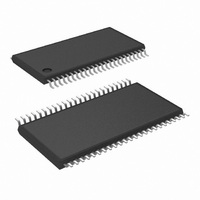
MCU 8BIT FLASH 8K MEM 48-TSSOP
Manufacturer
National Semiconductor
Series
COP8™ 8Cr
Datasheet
1.I2C-CPEV.pdf
(80 pages)
Specifications of COP8CCE9IMT7/NOPB
Core Processor
COP8
Core Size
8-Bit
Speed
10MHz
Connectivity
Microwire/Plus (SPI), UART/USART
Peripherals
Brown-out Detect/Reset, POR, PWM, WDT
Number Of I /o
39
Program Memory Size
8KB (8K x 8)
Program Memory Type
FLASH
Ram Size
256 x 8
Voltage - Supply (vcc/vdd)
2.7 V ~ 5.5 V
Data Converters
A/D 16x10b
Oscillator Type
Internal
Operating Temperature
-40°C ~ 125°C
Package / Case
48-TSSOP
Data Bus Width
8 bit
Maximum Clock Frequency
10 MHz
Data Ram Size
256 B
On-chip Adc
10 bit, 16 channel
Number Of Programmable I/os
37
Number Of Timers
2
Height
0.9 mm
Interface Type
SPI, USART
Length
12.5 mm
Maximum Operating Temperature
+ 125 C
Minimum Operating Temperature
- 40 C
Supply Voltage (max)
5.5 V
Supply Voltage (min)
2.7 V
Width
6.1 mm
Lead Free Status / RoHS Status
Lead free / RoHS Compliant
Eeprom Size
-
Lead Free Status / Rohs Status
Details
Other names
COP8CCE9IMT7


10.0 Functional Description
10.9.7 ENAD Register (Address X'00CB)
The ENAD register contains the following bits:
As described in Section 10.5 OPTION REGISTER, there is a
bit, FLEX, that controls whether the device exits RESET
executing from the flash memory or the Boot ROM. The user
must program the FLEX bit as appropriate for the applica-
tion. In the erased state, the FLEX bit = 0 and the device will
power-up executing from Boot ROM. When FLEX = 0, this
assumes that either the MICROWIRE/PLUS ISP routine or
external programming is being used to program the device. If
using the MICROWIRE/PLUS ISP routine, the software in
the boot ROM will monitor the MICROWIRE/PLUS for com-
mands to program the flash memory. When programming
the flash program memory is complete, the FLEX bit will
have to be programmed to a 1 and the device will have to be
reset, either by pulling external Reset to ground or by a
MICROWIRE/PLUS ISP EXIT command, before execution
from flash program memory will occur.
If FLEX = 1, upon exiting Reset, the device will begin ex-
ecuting from location 0000 in the flash program memory. The
assumption, here, is that either the application is not using
ADCH3 ADCH2
Bit 7
(Continued)
ADCH3 ADC channel select bit
ADCH2 ADC channel select bit
ADCH1 ADC channel select bit
ADCH0 ADC channel select bit
ADMOD Places the ADC in single-ended or differential
MUX
PSC
ADBSY Signifies that the ADC is currently busy perform-
Channel Select
mode.
Enables the ADC multiplexor output.
Switches the ADC clock between a divide by one
or a divide by sixteen of MCLK.
ing a conversion. When set by the user, starts a
conversion.
ADCH1
ADCH0
ADMOD
Select
Mode
Mux Out Prescale
MUX
FIGURE 13. Block Diagram of ISP
PSC
ADBSY
Busy
Bit 0
27
11.0 In-System Programming
11.1 INTRODUCTION
This device provides the capability to program the program
memory while installed in an application board. This feature
is called In System Programming (ISP). It provides a means
of ISP by using the MICROWIRE/PLUS, or the user can
provide his own, customized ISP routine. The factory in-
stalled ISP uses the MICROWIRE/PLUS port. The user can
provide his own ISP routine that uses any of the capabilities
of the device, such as USART, parallel port, etc.
11.2 FUNCTIONAL DESCRIPTION
The organization of the ISP feature consists of the user flash
program memory, the factory boot ROM, and some registers
dedicated to performing the ISP function. See Figure 13 for
a simplified block diagram. The factory installed ISP that
uses MICROWIRE/PLUS is located in the Boot ROM. The
size of the Boot ROM is 1k bytes and also contains code to
facilitate in system emulation capability. If a user chooses to
write his own ISP routine, it must be located in the flash
program memory.
ISP, is using MICROWIRE/PLUS ISP by jumping to it within
the application code, or is using a customized ISP routine. If
a customized ISP routine is being used, then it must be
programmed into the flash memory by means of the
MICROWIRE/PLUS ISP or external programming as de-
scribed in the preceding paragraph.
11.3 REGISTERS
There are six registers required to support ISP: Address
Register Hi byte (ISPADHI), Address Register Low byte
(ISPADLO), Read Data Register (ISPRD), Write Data Reg-
ister (ISPWR), Write Timing Register (PGMTIM), and the
Control Register (ISPCNTRL). The ISPCNTRL Register is
not available to the user.
11.3.1 ISP Address Registers
The address registers (ISPADHI & ISPADLO) are used to
specify the address of the byte of data being written or read.
For page erase operations, the address of the beginning of
20022517
www.national.com
Related parts for COP8CCE9IMT7/NOPB
Image
Part Number
Description
Manufacturer
Datasheet
Request
R

Part Number:
Description:
National Semiconductor [8-Bit D/A Converter]
Manufacturer:
National Semiconductor
Datasheet:
Part Number:
Description:
National Semiconductor [Media Coprocessor]
Manufacturer:
National Semiconductor
Datasheet:
Part Number:
Description:
Digitally Controlled Tone and Volume Circuit with Stereo Audio Power Amplifier, Microphone Preamp Stage and National 3D Sound
Manufacturer:
National Semiconductor
Datasheet:
Part Number:
Description:
Digitally Controlled Tone and Volume Circuit with Stereo Audio Power Amplifier, Microphone Preamp Stage and National 3D Sound
Manufacturer:
National Semiconductor
Datasheet:
Part Number:
Description:
AC97 Rev 2 Codec with Sample Rate Conversion and National 3D Sound
Manufacturer:
National Semiconductor
Part Number:
Description:
Manufacturer:
National Semiconductor
Datasheet:
Part Number:
Description:
Manufacturer:
National Semiconductor
Datasheet:
Part Number:
Description:
General Purpose, Low Voltage, Low Power, Rail-to-Rail Output Operational Amplifiers
Manufacturer:
National Semiconductor
Datasheet:
Part Number:
Description:
8-bit 20 MSPS flash A/D converter.
Manufacturer:
National Semiconductor
Datasheet:
Part Number:
Description:
Low Noise Quad Operational Amplifier
Manufacturer:
National Semiconductor
Datasheet:
Part Number:
Description:
Quad Differential Line Receivers
Manufacturer:
National Semiconductor
Datasheet:
Part Number:
Description:
Quad High Speed Trapezoidal? Bus Transceiver
Manufacturer:
National Semiconductor
Datasheet:
Part Number:
Description:
Dual Line Receiver
Manufacturer:
National Semiconductor
Datasheet:
Part Number:
Description:
TTL to 10k ECL Level Translator with Latch
Manufacturer:
National Semiconductor
Datasheet: