COP8CCE9IMT7/NOPB National Semiconductor, COP8CCE9IMT7/NOPB Datasheet - Page 30
COP8CCE9IMT7/NOPB
Manufacturer Part Number
COP8CCE9IMT7/NOPB
Description
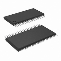
MCU 8BIT FLASH 8K MEM 48-TSSOP
Manufacturer
National Semiconductor
Series
COP8™ 8Cr
Datasheet
1.I2C-CPEV.pdf
(80 pages)
Specifications of COP8CCE9IMT7/NOPB
Core Processor
COP8
Core Size
8-Bit
Speed
10MHz
Connectivity
Microwire/Plus (SPI), UART/USART
Peripherals
Brown-out Detect/Reset, POR, PWM, WDT
Number Of I /o
39
Program Memory Size
8KB (8K x 8)
Program Memory Type
FLASH
Ram Size
256 x 8
Voltage - Supply (vcc/vdd)
2.7 V ~ 5.5 V
Data Converters
A/D 16x10b
Oscillator Type
Internal
Operating Temperature
-40°C ~ 125°C
Package / Case
48-TSSOP
Data Bus Width
8 bit
Maximum Clock Frequency
10 MHz
Data Ram Size
256 B
On-chip Adc
10 bit, 16 channel
Number Of Programmable I/os
37
Number Of Timers
2
Height
0.9 mm
Interface Type
SPI, USART
Length
12.5 mm
Maximum Operating Temperature
+ 125 C
Minimum Operating Temperature
- 40 C
Supply Voltage (max)
5.5 V
Supply Voltage (min)
2.7 V
Width
6.1 mm
Lead Free Status / RoHS Status
Lead free / RoHS Compliant
Eeprom Size
-
Lead Free Status / Rohs Status
Details
Other names
COP8CCE9IMT7


www.national.com
PGMTIM_SET
PAGE_ERASE
MASS_ERASE
READ_BYTE
11.0 In-System Programming
The correct sequence to be used to force execution from
Boot ROM is :
1. Disconnect G6 from the source of data for MICROWIRE/
2. Apply V
3. Pull RESET Low.
4. After V
5. Pull RESET High.
6. After a delay of at least three instruction cycles, remove
11.6 RETURN TO FLASH MEMORY WITHOUT
HARDWARE RESET
After programming the entire program memory, including
options, it is necessary to exit the Boot ROM and return to
the flash program memory for program execution. Upon
(Continued)
FIGURE 14. Circuit Diagram for Implementing the 2 x
PLUS ISP.
2 x V
time of the high voltage on G6 is slower than the mini-
mum in the Electrical Specifications. Figure 14 shows a
possible circuit dliagram for implementing the 2 x V
Be aware of the typical input current on the G6 pin when
the high voltage is applied. The resistor used in the RC
network, and the high voltage used, should be chosen to
keep the high voltage at the G6 pin between 2 x V
V
the high voltage from G6.
Command
CC
+7V.
CC
CC
CC
and V
is valid and stable, connect a voltage between
to the device.
CC
+7V to the G6 pin. Ensure that the rise
Write Pulse Timing
Register
Page Erase
Mass Erase
Read Byte
V
CC
Function
TABLE 10. MICROWIRE/PLUS ISP Commands
20022566
CC
and
CC
Value (Hex)
Command
.
0xBF
0x1D
0x3B
0xB3
30
receipt and completion of the EXIT command through the
MICROWIRE/PLUS ISP, the ISP code will reset the part and
begin execution from the flash program memory as de-
scribed in the Reset section. This assumes that the FLEX bit
in the Option register was programmed to 1.
11.7 MICROWIRE/PLUS ISP
National Semiconductor provides a program, which is avail-
able from our web site at www.national.com/cop8, that is
capable of programming a device from the parallel port of a
PC. The software accepts manually input commands and is
capable of downloading standard Intel HEX Format files.
Users who wish to write their own MICROWIRE/PLUS ISP
host software should refer to the COP8 FLASH ISP User
Manual, available from the same web site. This document
includes details of command format and delays necessary
between command bytes.
The MICROWIRE/PLUS ISP supports the following features
and commands:
• Write a value to the ISP Write Timing Register. NOTE:
• Erase the entire flash program memory (mass erase).
• Erase a page at a specified address.
• Read Option register.
• Read a byte from a specified address.
• Write a byte to a specified address.
• Read multiple bytes starting at a specified address.
• Write multiple bytes starting at a specified address.
• Exit ISP and return execution to flash program memory.
The following table lists the MICROWIRE/PLUS ISP com-
mands and provides information on required parameters and
return values.
This must be the first command after entering
MICROWIRE/PLUS ISP mode.
Value
Starting Address of
Page
Confirmation Code
Address High, Address
Low
Parameters
N/A
N/A
N/A (The entire Flash
Memory will be erased)
Data Byte if Security not
set. 0xFF if Security set.
Option Register if address
= 0xFFFF, regardless of
Security
Return Data
Related parts for COP8CCE9IMT7/NOPB
Image
Part Number
Description
Manufacturer
Datasheet
Request
R

Part Number:
Description:
National Semiconductor [8-Bit D/A Converter]
Manufacturer:
National Semiconductor
Datasheet:
Part Number:
Description:
National Semiconductor [Media Coprocessor]
Manufacturer:
National Semiconductor
Datasheet:
Part Number:
Description:
Digitally Controlled Tone and Volume Circuit with Stereo Audio Power Amplifier, Microphone Preamp Stage and National 3D Sound
Manufacturer:
National Semiconductor
Datasheet:
Part Number:
Description:
Digitally Controlled Tone and Volume Circuit with Stereo Audio Power Amplifier, Microphone Preamp Stage and National 3D Sound
Manufacturer:
National Semiconductor
Datasheet:
Part Number:
Description:
AC97 Rev 2 Codec with Sample Rate Conversion and National 3D Sound
Manufacturer:
National Semiconductor
Part Number:
Description:
Manufacturer:
National Semiconductor
Datasheet:
Part Number:
Description:
Manufacturer:
National Semiconductor
Datasheet:
Part Number:
Description:
General Purpose, Low Voltage, Low Power, Rail-to-Rail Output Operational Amplifiers
Manufacturer:
National Semiconductor
Datasheet:
Part Number:
Description:
8-bit 20 MSPS flash A/D converter.
Manufacturer:
National Semiconductor
Datasheet:
Part Number:
Description:
Low Noise Quad Operational Amplifier
Manufacturer:
National Semiconductor
Datasheet:
Part Number:
Description:
Quad Differential Line Receivers
Manufacturer:
National Semiconductor
Datasheet:
Part Number:
Description:
Quad High Speed Trapezoidal? Bus Transceiver
Manufacturer:
National Semiconductor
Datasheet:
Part Number:
Description:
Dual Line Receiver
Manufacturer:
National Semiconductor
Datasheet:
Part Number:
Description:
TTL to 10k ECL Level Translator with Latch
Manufacturer:
National Semiconductor
Datasheet: