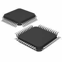
MAXQ7667AACM/V+T Maxim Integrated Products, MAXQ7667AACM/V+T Datasheet - Page 18

MAXQ7667AACM/V+T
Manufacturer Part Number
MAXQ7667AACM/V+T
Description
IC MCU-BASED DAS 16BIT 48-LQFP
Manufacturer
Maxim Integrated Products
Series
MAXQ™r
Datasheet
1.MAXQ7667AACMV.pdf
(40 pages)
Specifications of MAXQ7667AACM/V+T
Core Processor
RISC
Core Size
16-Bit
Speed
16MHz
Connectivity
LIN, SPI, UART/USART
Peripherals
Brown-out Detect/Reset, POR, WDT
Number Of I /o
16
Program Memory Size
32KB (16K x 16)
Program Memory Type
FLASH
Ram Size
2K x 16
Voltage - Supply (vcc/vdd)
2.25 V ~ 2.75 V
Data Converters
A/D 5x12b
Oscillator Type
Internal
Operating Temperature
-40°C ~ 125°C
Package / Case
48-LQFP
Processor Series
MAXQ7667
Core
RISC
Data Bus Width
16 bit
Data Ram Size
4 KB
Interface Type
UART, JTAG, LIN
Maximum Clock Frequency
16 MHz
Number Of Programmable I/os
16
Number Of Timers
3
Operating Supply Voltage
5 V
Maximum Operating Temperature
+ 125 C
Mounting Style
SMD/SMT
Development Tools By Supplier
MAXQ7667EVKIT
Minimum Operating Temperature
- 40 C
On-chip Adc
12 bit, 5 Channel
Lead Free Status / RoHS Status
Lead free / RoHS Compliant
Eeprom Size
-
Lead Free Status / Rohs Status
Details
16-Bit, RISC, Microcontroller-Based,
Ultrasonic Distance-Measuring System
The MAXQ7667 features a 16-bit sigma-delta ADC with
an analog gain adjustable from 38dB to 60dB (includ-
ing the fixed LNA gain) with a maximum gain step of
12.5% (typical). Gain changes settle within one ADC
conversion. Use software to create a virtual time vari-
able gain amplifier. A digital bandpass and lowpass fil-
ters remove switching glitches and DC offset at the
output of the ADC.
In a typical application, the software sets the gain to a
low value when the burst is first sent and increases the
gain as the time from when the burst was sent increas-
es. As a result, strong echoes from nearby objects are
processed without clipping while small signals from dis-
tant objects are processed with the maximum gain. The
ADC samples the amplified echo signal from the LNA at
80 times the burst output frequency. The ADC provides
conversion results at a data rate equal to 10 times the
burst output frequency. The ADC conversion results
also load to an 8-deep first-in-first-out (FIFO) at the
native data rate or a separate time base without loading
the CPU.
Figure 3. SAR ADC Block Diagram
18
AGND
AGND
AVDD
AIN0
AIN1
AIN2
AIN3
AIN4
______________________________________________________________________________________
V
REF
SARC[11:9]:SARMX[2:0]
OSCC[3:2]:SARCD[1:0]
SARC[2:0]:SARS[2:0]
SARC.6:SARDUL
SARC.4:SARASD
SARC.7:SARBIP
SARC.8:SARDIF
SARC.3:SARBY
MUX
SYSCLK
APE.4:SARE
CLOCK
ADC
DIV
AVDD
Sigma-Delta ADC
MUX
12-BIT
ADC
ADCCLK
V
REF
SARC[11:9]:SARMX[2:0]
SIGMA-DELTA ADC
DATA BUS[15:0]
REFERENCE TO
ASR.0:SARRDY
TIMER 0
TIMER 1
TIMER 2
The digital bandpass filter has a center frequency that
tracks the burst output frequency. The bandpass width
is 14% of the center frequency. The bandpass filter pro-
vides the 16-bit output data at a data rate equal to 10
times the burst output frequency.
The full-wave rectifier detects the envelope of the digital
bandwidth filter output to generate a DC output propor-
tional to the peak-to-peak amplitude of the input signal.
Full-wave rectification allows the digital lowpass filter to
respond faster without excessive ripple.
The lowpass filter removes the ripple from the full-wave
detector output. The output of the lowpass filter is avail-
able at a data rate equal to five times the burst output
frequency. The corner frequency is 1/5 the burst fre-
quency with approximately 40dB per decade rolloff.
The 16-bit output data of the lowpass filter is stored in a
FIFO register with a depth of eight samples. The
MAXQ7667 allows data transfer from the lowpass filter
APE.14:RBUFE
APE.12:BGE
AIE.0:SARIE
BUF
x1.0
BANDGAP
REF
Digital Bandpass Filter
Digital Lowpass Filter
ADC DATA
READY INTERRUPT
Full-Wave Rectifier
REF
REFBG
ADCCTL


