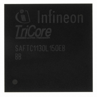
SAF-TC1130-L150EB-G BB Infineon Technologies, SAF-TC1130-L150EB-G BB Datasheet - Page 91

SAF-TC1130-L150EB-G BB
Manufacturer Part Number
SAF-TC1130-L150EB-G BB
Description
IC MCU 32BIT TRICOR 16KB LBGA208
Manufacturer
Infineon Technologies
Series
TC11xxr
Datasheet
1.SAF-TC1130-L100EB-G_BB.pdf
(114 pages)
Specifications of SAF-TC1130-L150EB-G BB
Core Processor
TriCore
Core Size
32-Bit
Speed
150MHz
Connectivity
CAN, EBI/EMI, FIFO, I²C, IrDA, SPI, UART/USART, USB
Peripherals
DMA, POR, PWM, WDT
Number Of I /o
72
Program Memory Type
ROMless
Ram Size
144K x 8
Voltage - Supply (vcc/vdd)
1.43 V ~ 1.58 V
Oscillator Type
External
Operating Temperature
-40°C ~ 85°C
Package / Case
208-LSBGA
Data Bus Width
32 bit
Program Memory Size
32 KB
Data Ram Size
144 KB
Interface Type
3xASC, 2xSSC, I2C, 2xMLI, Ethernet 10, 100 Mbits, s, USB
Maximum Clock Frequency
150 MHz
Number Of Programmable I/os
72
Number Of Timers
9
Operating Supply Voltage
1.5 V, 3.3 V
Maximum Operating Temperature
+ 85 C
Mounting Style
SMD/SMT
Minimum Operating Temperature
- 40 C
Packages
PG-LBGA-208
Max Clock Frequency
150.0 MHz
Sram (incl. Cache)
144.0 KByte
Can Nodes
4
Program Memory
0.0 KByte
Lead Free Status / RoHS Status
Lead free / RoHS Compliant
Eeprom Size
-
Program Memory Size
-
Data Converters
-
Lead Free Status / Rohs Status
Details
Other names
FT1130L150EBGBBXP
SAF-TC1130-L150EB-GBB
SAF-TC1130-L150EB-GBBINTR
SAF-TC1130-L150EB-GBBTR
SAF-TC1130-L150EB-GBBTR
SAFTC1130L150EBBBXT
SP000106119
SP000106538
SP000743584
SAF-TC1130-L150EB-GBB
SAF-TC1130-L150EB-GBBINTR
SAF-TC1130-L150EB-GBBTR
SAF-TC1130-L150EB-GBBTR
SAFTC1130L150EBBBXT
SP000106119
SP000106538
SP000743584
4.3.2
When PLL operation is configured (PLL_CLC.LOCK = 1), the on-chip phase locked loop
is enabled and provides the master clock. The PLL multiplies the input frequency by the
factor F (
Factor), and the output divider (F = NDIV+1 / (PDIV+1
synchronizes the master clock to the input clock. This synchronization is done smoothly,
i.e. the master clock frequency does not change abruptly.
Due to this adaptation to the input clock, the frequency of
it is locked to
duration of individual TCMs.
The timing listed in the AC Characteristics refers to TCPs. Because
f
circumstances.
The actual minimum value for TCP depends on the jitter of the PLL. As the PLL is
constantly adjusting its output frequency in order to correspond to the applied input
frequency (crystal or oscillator), the relative deviation for periods of more than one TCP
is lower than for one single TCP (see formula and
This is especially important for bus cycles using waitstates and for the operation of
timers, serial interfaces, etc. For all slower operations and longer periods (e.g. pulse train
generation or measurement, lower baud rates, etc.) the deviation caused by the PLL
jitter is negligible.
The value of the accumulated PLL jitter depends on the number of consecutive VCO
output cycles within the respective timeframe. The VCO output clock is divided by the
output prescaler (K = KDIV+1) to generate the master clock signal
number of VCO cycles can be represented as K ×
consecutive
For a period of
deviation D
D
So, for a period of 3 TCMs @ 20 MHz and K = 12: D
This formula is applicable for K ×
used. This steady value can be approximated by: D
Data Sheet
MC
N
, the timing must be calculated using the minimum TCP possible under the respective
[ns] = ±(1.5 + 6.32 ×
f
MC
N
PLL Parameters
f
:
=
MC
f
f
OSC
OSC
N
cycles (TCM).
× TCM, the accumulated PLL jitter is defined by the corresponding
. The slight variation causes a jitter of
× F) which results from the input divider, the multiplication factor (N
N
/
f
MC
);
N
f
MC
< 95. For longer periods, the K×
in [MHz],
85
N
= number of consecutive TCMs.
Figure
3
Nmax
= ±(1.5 + 6.32 ×
N
, where
[ns] = ±(1.5 + 600 / (K ×
4-3).
×
f
MC
f
KDIV+1)). The PLL circuit
MC
is constantly adjusted so
Electrical Parameters
which also affects the
N
f
f
N
CPU
MC
is the number of
3
=95 value can be
/ 20) = 2.448 ns.
. Therefore, the
is derived from
V1.1, 2008-12
TC1130
f
MC
)).


