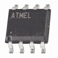
AT90LS2323-4SI Atmel, AT90LS2323-4SI Datasheet - Page 26

AT90LS2323-4SI
Manufacturer Part Number
AT90LS2323-4SI
Description
IC MCU 2K FLASH 4MHZ LV 8-SOIC
Manufacturer
Atmel
Series
AVR® 90LSr
Datasheet
1.AT90LS2323-4PC.pdf
(64 pages)
Specifications of AT90LS2323-4SI
Core Processor
AVR
Core Size
8-Bit
Speed
4MHz
Connectivity
SPI
Peripherals
Brown-out Detect/Reset, POR, WDT
Number Of I /o
3
Program Memory Size
2KB (1K x 16)
Program Memory Type
FLASH
Eeprom Size
128 x 8
Ram Size
128 x 8
Voltage - Supply (vcc/vdd)
2.7 V ~ 6 V
Oscillator Type
Internal
Operating Temperature
-40°C ~ 85°C
Package / Case
8-SOIC (5.3mm Width), 8-SOP, 8-SOEIAJ
Lead Free Status / RoHS Status
Contains lead / RoHS non-compliant
Data Converters
-
Available stocks
Company
Part Number
Manufacturer
Quantity
Price
Part Number:
AT90LS2323-4SI
Manufacturer:
ATMEL/爱特梅尔
Quantity:
20 000
External Interrupt
Interrupt Response Time
MCU Control Register –
MCUCR
26
AT90S/LS2323/2343
• Bit 0 – Res: Reserved Bit
This bit is a reserved bit in the AT90S2323/2343 and always reads zero.
The external interrupt is triggered by the INT0 pin. Observe that, if enabled, the interrupt
will trigger even if the INT0 pin is configured as an output. This feature provides a way of
generating a software interrupt. The external interrupt can be triggered by a falling or ris-
ing edge or a low level. This is set up as indicated in the specification for the MCU
Control Register (MCUCR). When the external interrupt is enabled and is configured as
level-triggered, the interrupt will trigger as long as the pin is held low.
The external interrupt is set up as described in the specification for the MCU Control
Register (MCUCR).
The interrupt execution response for all the enabled AVR interrupts is four clock cycles
minimum. Four clock cycles after the interrupt flag has been set, the program vector
address for the actual interrupt handling routine is executed. During these four clock
cycles, the Program Counter (2 bytes) is popped back from the stack, the Stack Pointer
is incremented by 2 and the I-flag in SREG is set. The vector is a relative jump to the
interrupt routine and this jump takes two clock cycles. If an interrupt occurs during exe-
cution of a multi-cycle instruction, this instruction is completed before the interrupt is
served.
A return from an interrupt handling routine (same as for a subroutine call routine) takes
four clock cycles. During these four clock cycles, the Program Counter (2 bytes) is
popped back from the stack and the Stack Pointer is incremented by 2. When the AVR
exits from an interrupt, it will always return to the main program and execute one more
instruction before any pending interrupt is served.
The MCU Control Register contains control bits for general MCU functions.
• Bits 7, 6 – Res: Reserved Bits
These bits are reserved bits in the AT90S2323/2343 and always read as zero.
• Bit 5 – SE: Sleep Enable
The SE bit must be set (one) to make the MCU enter the Sleep mode when the SLEEP
instruction is executed. To avoid the MCU entering the Sleep mode, unless it is the pro-
grammer’s purpose, it is recommended to set the Sleep Enable (SE) bit just before the
execution of the SLEEP instruction.
• Bit 4 – SM: Sleep Mode
This bit selects between the two available sleep modes. When SM is cleared (zero), Idle
mode is selected as Sleep mode. When SM is set (one), Power-down mode is selected
as sleep mode. For details, refer to the section “Sleep Modes”.
• Bits 3, 2 – Res: Reserved Bits
These bits are reserved bits in the AT90S2323/2343 and always read as zero.
• Bits 1, 0 – ISC01, ISC00: Interrupt Sense Control 0 Bit 1 and Bit 0
The External Interrupt 0 is activated by the external pin INT0 if the SREG I-flag and the
corresponding interrupt mask are set. The level and edges on the external INT0 pin that
Bit
$35 ($55)
Read/Write
Initial Value
R
7
–
0
R
6
–
0
R/W
SE
5
0
R/W
SM
4
0
R
3
–
0
R
2
–
0
ISC01
R/W
1
0
ISC00
R/W
0
0
1004D–09/01
MCUCR


