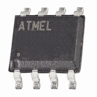
AT90LS2323-4SI Atmel, AT90LS2323-4SI Datasheet - Page 40

AT90LS2323-4SI
Manufacturer Part Number
AT90LS2323-4SI
Description
IC MCU 2K FLASH 4MHZ LV 8-SOIC
Manufacturer
Atmel
Series
AVR® 90LSr
Datasheet
1.AT90LS2323-4PC.pdf
(64 pages)
Specifications of AT90LS2323-4SI
Core Processor
AVR
Core Size
8-Bit
Speed
4MHz
Connectivity
SPI
Peripherals
Brown-out Detect/Reset, POR, WDT
Number Of I /o
3
Program Memory Size
2KB (1K x 16)
Program Memory Type
FLASH
Eeprom Size
128 x 8
Ram Size
128 x 8
Voltage - Supply (vcc/vdd)
2.7 V ~ 6 V
Oscillator Type
Internal
Operating Temperature
-40°C ~ 85°C
Package / Case
8-SOIC (5.3mm Width), 8-SOP, 8-SOEIAJ
Lead Free Status / RoHS Status
Contains lead / RoHS non-compliant
Data Converters
-
Available stocks
Company
Part Number
Manufacturer
Quantity
Price
Part Number:
AT90LS2323-4SI
Manufacturer:
ATMEL/爱特梅尔
Quantity:
20 000
Table 16. High-voltage Serial Programming Instruction Set
40
Instruction
Chip Erase
Write Flash
High and Low
Address
Write Flash
Low Byte
Write Flash
High Byte
Read Flash
High and Low
Address
Read Flash
Low Byte
Read Flash
High Byte
Write
EEPROM
Low Address
Write
EEPROM
Byte
Read
EEPROM
Low Address
Read
EEPROM
Byte
Write Fuse
Bits (AT90S/
LS2323)
Write Fuse
Bits (AT90S/
LS2343)
Write Lock
Bits
AT90S/LS2323/2343
PB0
PB1
PB2
PB0
PB1
PB2
PB0
PB1
PB2
PB0
PB1
PB2
PB0
PB1
PB2
PB0
PB1
PB2
PB0
PB1P
B2
PB0
PB1
PB2
PB0
PB1
PB2
PB0
PB1
PB2
PB0
PB1
PB2
PB0
PB1
PB2
PB0
PB1
PB2
PB0
PB1
PB2
0_1000_0000_00
0_0100_1100_00
0_0001_0000_00
0_0100_1100_00
0_ i i i i_i i i i _00
0_0010_1100_00
0_ i i i i_i i i i _00
0_0010_1100_00
0_0000_0010_00
0_0100_1100_00
0_0000_0000_00
0_0110_1000_00
0_0000_0000_00
0_0111_1000_00
0_0001_0001_00
0_0100_1100_00
0_ i i i i_i i i i _00
0_0010_1100_00
0_0000_0011_00
0_0100_1100_00
0_0000_0000_00
0_0110_1000_00
0_0100_0000_00
0_0100_1100_00
0_0100_0000_00
0_0100_1100_00
0_0010_0000_00
0_0100_1100_00
x_xxxx_xxxx_xx
x_xxxx_xxxx_xx
x_xxxx_xxxx_xx
x_xxxx_xxxx_xx
x_xxxx_xxxx_xx
x_xxxx_xxxx_xx
x_xxxx_xxxx_xx
x_xxxx_xxxx_xx
x_xxxx_xxxx_xx
x_xxxx_xxxx_xx
x_xxxx_xxxx_xx
x_xxxx_xxxx_xx
x_xxxx_xxxx_xx
x_xxxx_xxxx_xx
Instr.1
0_0bbb_bbbb_00
0_0bbb_bbbb_00
0_11S1_111R_00
o_oooo_ooox_xx
o_oooo_ooox_xx
o_oooo_ooox_xx
0_11S1_111F_00
0_0000_0000_00
0_0110_0100_00
0_0000_00aa_00
0_0001_1100_00
0_0000_0000_00
0_0110_0100_00
0_0000_0000_00
0_0111_0100_00
0_0000_00aa_00
0_0001_1100_00
0_0000_0000_00
0_0110_1100_00
0_0000_0000_00
0_0111_1100_00
0_0000_1100_00
0_0000_0000_00
0_0110_0100_00
0_0000_1100_00
0_0000_0000_00
0_0110_1100_00
0_0010_1100_00
0_0010_1100_00
0_1111_1211_00
0_0010_1100_00
x_xxxx_xxxx_xx
x_xxxx_xxxx_xx
x_xxxx_xxxx_xx
x_xxxx_xxxx_xx
x_xxxx_xxxx_xx
x_xxxx_xxxx_xx
x_xxxx_xxxx_xx
x_xxxx_xxxx_xx
x_xxxx_xxxx_xx
x_xxxx_xxxx_xx
x_xxxx_xxxx_xx
Instr.2
Instruction Format
0_bbbb_bbbb_00
0_bbbb_bbbb_00
0_0000_0000_00
0_0110_1100_00
0_0000_1100_00
0_0000_0000_00
0_0110_1100_00
0_0000_0000_00
0_0000_0000_00
0_0111_1100_00
0_0000_0000_00
0_0000_1100_00
0_0000_0000_00
0_0110_1100_00
0_0000_0000_00
0_0000_0000_00
0_0110_0100_00
0_0000_0000_00
0_0110_0100_00
0_0000_0000_00
0_0110_0100_00
x_xxxx_xxxx_xx
x_xxxx_xxxx_xx
x_xxxx_xxxx_xx
x_xxxx_xxxx_xx
x_xxxx_xxxx_xx
x_xxxx_xxxx_xx
Instr.3
0_0000_0000_00
0_0100_1100_00
0_0000_0000_00
0_0110_1100_00
0_0000_0000_00
0_0110_1100_00
0_0000_0000_00
0_0110_1100_00
0_0000_0000_00
x_xxxx_xxxx_xx
x_xxxx_xxxx_xx
x_xxxx_xxxx_xx
Instr.4
Operation Remarks
Wait t
the Chip Erase cycle to finish.
Repeat Instr.2 for a new
256-byte page. Repeat Instr.3
for each new address.
Wait after Instr.3 until PB2
goes high. Repeat Instr.1,
Instr. 2 and Instr.3 for each
new address.
Wait after Instr.3 until PB2
goes high. Repeat Instr.1,
Instr. 2 and Instr.3 for each
new address.
Repeat Instr.2 and Instr.3 for
each new address.
Repeat Instr.1 and Instr.2 for
each new address.
Repeat Instr.1 and Instr.2 for
each new address.
Repeat Instr.2 for each new
address.
Wait after Instr.3 until PB2
goes high
Repeat Instr.2 for each new
address.
Repeat Instr.2 for each new
address
Wait t
the Write Fuse bits cycle to
finish. Set S,F = “0” to
program, “1” to unprogram.
Wait t
the Write Fuse bits cycle to
finish. Set S,R = “0” to
program, “1” to unprogram.
Wait after Instr.4 until PB2
goes high. Write 2, 1 = “0” to
program the Lock bit.
WLWH_CE
WLWH_PFB
WLWH_PFB
after Instr.3 for
after Instr.3 for
after Instr.3 for
1004D–09/01


