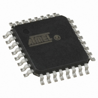
ATTINY28V-1AC Atmel, ATTINY28V-1AC Datasheet - Page 25

ATTINY28V-1AC
Manufacturer Part Number
ATTINY28V-1AC
Description
IC AVR MCU 2K 1.2MHZ 1.8V 32TQFP
Manufacturer
Atmel
Series
AVR® ATtinyr
Specifications of ATTINY28V-1AC
Core Processor
AVR
Core Size
8-Bit
Speed
1.2MHz
Peripherals
POR, WDT
Number Of I /o
11
Program Memory Size
2KB (1K x 16)
Program Memory Type
FLASH
Voltage - Supply (vcc/vdd)
1.8 V ~ 5.5 V
Oscillator Type
Internal
Operating Temperature
0°C ~ 70°C
Package / Case
32-TQFP, 32-VQFP
Lead Free Status / RoHS Status
Contains lead / RoHS non-compliant
Eeprom Size
-
Ram Size
-
Data Converters
-
Connectivity
-
Available stocks
Company
Part Number
Manufacturer
Quantity
Price
I/O Ports
Port A
Port A as General Digital I/O
Alternate Function of PA2
1062F–AVR–07/06
All AVR ports have true read-modify-write functionality when used as general digital I/O
ports. This means that the direction of one port pin can be changed without unintention-
ally changing the direction of any other pin with the SBI and CBI instructions. The same
applies for changing drive value (if configured as output) or enabling/disabling of pull-up
resistors (if configured as input).
Port A is a 4-bit I/O port. PA3, PA1, and PA0 are bi-directional, while PA2 is output-only.
Before entering Power-down, see “Sleep Modes” on page 14, PORTA2 bit in PORTA
register should be set.
Three I/O memory address locations are allocated for Port A, one each for the Data
Register – PORTA, $1B, Port A Control Register – PACR, $1A and the Port A Input Pins
– PINA, $19. The Port A Input Pins address is read-only, while the Data Register and
the Control Register are read/write. Compared to other output ports, the Port A output is
delayed one extra clock cycle.
Port pins PA0, PA1 and PA3 have individually selectable pull-up resistors. When pins
PA0, PA1 or PA3 are used as inputs and are externally pulled low, they will source cur-
rent if the internal pull-up resistors are activated. PA2 is output-only. The PA2 output
buffer can sink 25 mA and thus drive a high-current LED directly. This output can also
be modulated (see “Hardware Modulator” on page 39 for details).
PA3, PA1 and PA0 are general I/O pins. The DDAn (n: 3,1,0) bits in PACR select the
direction of these pins. If DDAn is set (one), PAn is configured as an output pin. If DDAn
is cleared (zero), PAn is configured as an input pin. If PORTAn is set (one) when the pin
is configured as an input pin, the MOS pull-up resistor is activated. To switch the pull-up
resistor off, the PORTAn bit has to be cleared (zero) or the pin has to be configured as
an output pin. The effects of the DDAn and PORTAn bits on PA3, PA1 and PA0 are
shown in Table 10. The port pins are tri-stated when a reset condition becomes active,
even if the clock is not running.
Table 10. DDAn Effects on Port A Pins
Note:
PA2 is the built-in, high-current LED driver and it is always an output pin. The output sig-
nal can be modulated with a software programmable frequency. See “Hardware
Modulator” on page 39 for further details.
DDAn
0
0
1
1
n: 3,1,0, pin number
PORTAn
0
1
0
1
Output
Output
Input
Input
I/O
Pull-up
Yes
No
No
No
Comment
Tri-state (high-Z)
PAn will source current if ext. pulled low.
Push-pull Zero Output
Push-pull One Output
ATtiny28L/V
25


