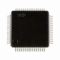
LPC2194JBD64,151 NXP Semiconductors, LPC2194JBD64,151 Datasheet - Page 18

LPC2194JBD64,151
Manufacturer Part Number
LPC2194JBD64,151
Description
IC ARM7 MCU FLASH 256K 64-LQFP
Manufacturer
NXP Semiconductors
Series
LPC2100r
Datasheet
1.LPC2194JBD64151.pdf
(33 pages)
Specifications of LPC2194JBD64,151
Core Processor
ARM7
Core Size
16/32-Bit
Speed
60MHz
Connectivity
CAN, I²C, Microwire, SPI, SSI, SSP, UART/USART
Peripherals
POR, PWM, WDT
Number Of I /o
46
Program Memory Size
256KB (256K x 8)
Program Memory Type
FLASH
Ram Size
16K x 8
Voltage - Supply (vcc/vdd)
1.65 V ~ 3.6 V
Data Converters
A/D 4x10b
Oscillator Type
Internal
Operating Temperature
-40°C ~ 105°C
Package / Case
64-LQFP
Lead Free Status / RoHS Status
Lead free / RoHS Compliant
Eeprom Size
-
Other names
568-1895
935275729151
LPC2194JBD64-S
935275729151
LPC2194JBD64-S
Available stocks
Company
Part Number
Manufacturer
Quantity
Price
Company:
Part Number:
LPC2194JBD64,151
Manufacturer:
NXP Semiconductors
Quantity:
10 000
Philips Semiconductors
9397 750 12757
Preliminary data
6.14.1 Features
6.15.1 Features
6.16.1 Features
6.15 SPI serial I/O controller
6.16 General purpose timers
I
The LPC2194 contains two SPIs. The SPI is a full duplex serial interface, designed to
be able to handle multiple masters and slaves connected to a given bus. Only a single
master and a single slave can communicate on the interface during a given data
transfer. During a data transfer the master always sends a byte of data to the slave,
and the slave always sends a byte of data to the master.
The Timer is designed to count cycles of the peripheral clock (PCLK) and optionally
generate interrupts or perform other actions at specified timer values, based on four
match registers. It also includes four capture inputs to trap the timer value when an
input signal transitions, optionally generating an interrupt. Multiple pins can be
selected to perform a single capture or match function, providing an application with
‘or’ and ‘and’, as well as ‘broadcast’ functions among them.
2
•
•
•
•
•
•
•
•
•
•
•
•
•
•
C implemented in LPC2194 supports bit rate up to 400 kbit/s (Fast I
Standard I
Easy to configure as Master, Slave, or Master/Slave.
Programmable clocks allow versatile rate control.
Bidirectional data transfer between masters and slaves.
Multi-master bus (no central master).
Arbitration between simultaneously transmitting masters without corruption of
serial data on the bus.
Serial clock synchronization allows devices with different bit rates to communicate
via one serial bus.
Serial clock synchronization can be used as a handshake mechanism to suspend
and resume serial transfer.
The I
Compliant with Serial Peripheral Interface (SPI) specification.
Synchronous, Serial, Full Duplex, Communication.
Combined SPI master and slave.
Maximum data bit rate of one eighth of the input clock rate.
A 32-bit Timer/Counter with a programmable 32-bit Prescaler.
2
C bus may be used for test and diagnostic purposes.
2
C compliant bus interface.
Rev. 01 — 06 February 2004
Single-chip 16/32-bit microcontrollers
© Koninklijke Philips Electronics N.V. 2004. All rights reserved.
LPC2194
2
C).
18 of 33


