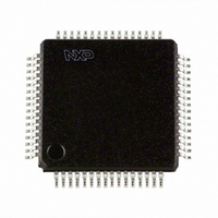
LPC2194JBD64,151 NXP Semiconductors, LPC2194JBD64,151 Datasheet - Page 26

LPC2194JBD64,151
Manufacturer Part Number
LPC2194JBD64,151
Description
IC ARM7 MCU FLASH 256K 64-LQFP
Manufacturer
NXP Semiconductors
Series
LPC2100r
Datasheet
1.LPC2194JBD64151.pdf
(33 pages)
Specifications of LPC2194JBD64,151
Core Processor
ARM7
Core Size
16/32-Bit
Speed
60MHz
Connectivity
CAN, I²C, Microwire, SPI, SSI, SSP, UART/USART
Peripherals
POR, PWM, WDT
Number Of I /o
46
Program Memory Size
256KB (256K x 8)
Program Memory Type
FLASH
Ram Size
16K x 8
Voltage - Supply (vcc/vdd)
1.65 V ~ 3.6 V
Data Converters
A/D 4x10b
Oscillator Type
Internal
Operating Temperature
-40°C ~ 105°C
Package / Case
64-LQFP
Lead Free Status / RoHS Status
Lead free / RoHS Compliant
Eeprom Size
-
Other names
568-1895
935275729151
LPC2194JBD64-S
935275729151
LPC2194JBD64-S
Available stocks
Company
Part Number
Manufacturer
Quantity
Price
Company:
Part Number:
LPC2194JBD64,151
Manufacturer:
NXP Semiconductors
Quantity:
10 000
Philips Semiconductors
Table 10:
T
[1]
[2]
[3]
[4]
[5]
[6]
[7]
[8]
Table 11:
V
4.5 MHz.
[1]
[2]
[3]
[4]
[5]
[6]
[7]
9397 750 12757
Preliminary data
Symbol Parameter
V
V
I
Oscillator pins
Symbol
AV
C
DL
IL
OS
G
A
lkg
amb
3A
hys
OL
e
IN
e
e
IN
e
e
= 2.5 V to 3.6 V unless otherwise specified; T
Typical ratings are not guaranteed. The values listed are at room temperature (+25 ˚C), nominal supply voltages.
Pin capacitance is characterized but not tested.
Including voltage on outputs in 3-state mode.
V
3-state outputs go into 3-state mode when V
Accounts for 100 mV voltage drop in all supply lines.
Only allowed for a short time period.
Minimum condition for V
Conditions: V
The A/D is monotonic, there are no missing codes.
The differential non-linearity (DLe) is the difference between the actual step width and the ideal step width. See
The integral no-linearity (ILe) is the peak difference between the center of the steps of the actual and the ideal transfer curve after
appropriate adjustment of gain and offset errors. See
The offset error (OSe) is the absolute difference between the straight line which fits the actual curve and the straight line which fits the
ideal curve. See
The gain error (Ge) is the relative difference in percent between the straight line fitting the actual transfer curve after removing offset
error, and the straight line which fits the ideal transfer curve. See
The absolute voltage error (Ae) is the maximum difference between the center of the steps of the actual transfer curve of the
non-calibrated A/D and the ideal transfer curve. See
= 40 C to +85 C for commercial, unless otherwise specified.
3
supply voltages must be present.
Hysteresis voltage
Low level output voltage
Input leakage to V
X1 input Voltages
X2 output Voltages
Static characteristics
A/D converter DC electrical characteristics
SSA
Parameter
Analog input voltage
Analog input capacitance
Differential non-linearity
Integral non-linearity
Offset error
Gain error
Absolute error
Figure
= 0 V, V
4.
i
= 4.5 V, maximum condition for V
3A
[1][6]
SS
[1][5]
= 3.3 V.
[1][7]
[6]
…continued
[1][4]
Conditions
V
I
V
V
[1][2][3]
OL
TOL
i
i
= V
= 5 V
3
= 3 mA
is grounded.
is from 4.5 V to 5.5 V
3
amb
Rev. 01 — 06 February 2004
Figure
Figure
= 40 C to +85 C unless otherwise specified; A/D converter frequency
i
= 5.5 V.
4.
4.
Figure
4.
Min
0
-
-
-
-
-
-
Min
-
-
-
-
0
0
Single-chip 16/32-bit microcontrollers
© Koninklijke Philips Electronics N.V. 2004. All rights reserved.
Max
V
1
Typ
0.5 V
-
2
10
-
-
1
2
3
0.5
4
3A
[1]
TOL
LPC2194
Figure
Max
-
0.4
4
22
V
V
18
18
Unit
V
pF
LSB
LSB
LSB
%
LSB
4.
26 of 33
Unit
V
V
A
A


