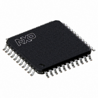
P89CV51RC2FBC,557 NXP Semiconductors, P89CV51RC2FBC,557 Datasheet - Page 18

P89CV51RC2FBC,557
Manufacturer Part Number
P89CV51RC2FBC,557
Description
IC 80C51 MCU FLASH 64K 44-TQFP
Manufacturer
NXP Semiconductors
Series
89Cr
Datasheet
1.P89CV51RB2FA512.pdf
(76 pages)
Specifications of P89CV51RC2FBC,557
Program Memory Type
FLASH
Program Memory Size
32KB (32K x 8)
Package / Case
44-TQFP, 44-VQFP
Core Processor
8051
Core Size
8-Bit
Speed
40MHz
Connectivity
EBI/EMI, SPI, UART/USART
Peripherals
POR, PWM, WDT
Number Of I /o
32
Ram Size
1K x 8
Voltage - Supply (vcc/vdd)
4.5 V ~ 5.5 V
Oscillator Type
Internal
Operating Temperature
-40°C ~ 85°C
Processor Series
P89CV5x
Core
80C51
Data Bus Width
8 bit
Data Ram Size
1 KB
Interface Type
SPI/UART
Maximum Clock Frequency
40 MHz
Number Of Programmable I/os
32
Number Of Timers
3
Operating Supply Voltage
4.5 V to 5.5 V
Maximum Operating Temperature
+ 85 C
Mounting Style
SMD/SMT
3rd Party Development Tools
PK51, CA51, A51, ULINK2
Minimum Operating Temperature
- 40 C
Lead Free Status / RoHS Status
Lead free / RoHS Compliant
Eeprom Size
-
Data Converters
-
Lead Free Status / Rohs Status
Lead free / RoHS Compliant
Other names
568-4255
935284104557
P89CV51RC2FBC
935284104557
P89CV51RC2FBC
Available stocks
Company
Part Number
Manufacturer
Quantity
Price
Company:
Part Number:
P89CV51RC2FBC,557
Manufacturer:
NXP Semiconductors
Quantity:
10 000
NXP Semiconductors
Table 10.
P89CV51RB2_RC2_RD2_3
Product data sheet
Device
P89CV51RB2/RC2/RD2
Default boot vector values and ISP entry points
6.3.3 Boot block
6.3.4 Power-on reset code execution
6.3.5 Hardware activation of the bootloader
6.3.6 ISP
When the microcontroller programs its own flash memory, all of the low-level details are
handled by code (bootloader) that is contained in a boot block. A user program calls the
common entry point in the boot block with appropriate parameters to accomplish the
desired operation. Boot block operations include erase user code, program user code,
program security bits, chip erase, etc. The boot block logically overlays the program
memory space from FC00H to FFFFH, when it is enabled. The boot block may be
disabled on-the-fly so that the upper 1 kB of user code is available to the user’s program.
The P89CV51RB2/RC2/RD2 contains two special flash elements: the boot vector and the
boot status bit. Following reset, the P89CV51RB2/RC2/RD2 examines the contents of the
boot status bit. If the boot status bit is set to zero, power-up execution starts at location
0000H, which is the normal start address of the user’s application code. When the boot
status bit is set to a value other than zero, the contents of the boot vector are used as the
high byte of the execution address and the low byte is set to 00H.
Table 10
bootloader is pre-programmed into the address space indicated and uses the indicated
bootloader entry point to perform ISP functions.
The bootloader can also be executed by forcing the device into ISP mode during a
power-on sequence. This has the same effect as having a non-zero status byte. This
allows an application to be built that will normally execute user code but can be manually
forced into ISP operation. This occurs by holding PSEN LOW at the falling edge of reset. If
the factory default setting for the boot vector (FCH) is changed, it will no longer point to the
factory pre-programmed ISP bootloader code. After programming the flash, the status
byte should be programmed to zero in order to allow execution of the user’s application
code beginning at address 0000H.
ISP is performed without removing the microcontroller from the system. The ISP facility
consists of a series of internal hardware resources coupled with internal firmware to
facilitate remote programming of the P89CV51RB2/RC2/RD2 through the serial port. This
firmware is provided by NXP and embedded within each P89CV51RB2/RC2/RD2 device.
The NXP ISP facility has made in-circuit programming in an embedded application
possible with a minimum of additional expense in components and circuit board area. The
ISP function uses five pins (V
needs to be available to interface your application to an external circuit in order to use this
feature.
•
•
•
Default boot vector
FCH
Programming with industry-standard commercial programmers.
10000 typical erase/program cycles for each byte.
100 year minimum data retention.
shows the factory default boot vector setting for this device. A factory-provided
Rev. 03 — 25 August 2009
Default bootloader entry point
FC00H
DD
, V
SS
, TXD, RXD, and RST). Only a small connector
P89CV51RB2/RC2/RD2
Default bootloader code range
FC00H to FFFFH
80C51 with 1 kB RAM, SPI
© NXP B.V. 2009. All rights reserved.
18 of 76


