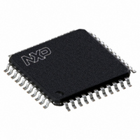
P89CV51RC2FBC,557 NXP Semiconductors, P89CV51RC2FBC,557 Datasheet - Page 36

P89CV51RC2FBC,557
Manufacturer Part Number
P89CV51RC2FBC,557
Description
IC 80C51 MCU FLASH 64K 44-TQFP
Manufacturer
NXP Semiconductors
Series
89Cr
Datasheet
1.P89CV51RB2FA512.pdf
(76 pages)
Specifications of P89CV51RC2FBC,557
Program Memory Type
FLASH
Program Memory Size
32KB (32K x 8)
Package / Case
44-TQFP, 44-VQFP
Core Processor
8051
Core Size
8-Bit
Speed
40MHz
Connectivity
EBI/EMI, SPI, UART/USART
Peripherals
POR, PWM, WDT
Number Of I /o
32
Ram Size
1K x 8
Voltage - Supply (vcc/vdd)
4.5 V ~ 5.5 V
Oscillator Type
Internal
Operating Temperature
-40°C ~ 85°C
Processor Series
P89CV5x
Core
80C51
Data Bus Width
8 bit
Data Ram Size
1 KB
Interface Type
SPI/UART
Maximum Clock Frequency
40 MHz
Number Of Programmable I/os
32
Number Of Timers
3
Operating Supply Voltage
4.5 V to 5.5 V
Maximum Operating Temperature
+ 85 C
Mounting Style
SMD/SMT
3rd Party Development Tools
PK51, CA51, A51, ULINK2
Minimum Operating Temperature
- 40 C
Lead Free Status / RoHS Status
Lead free / RoHS Compliant
Eeprom Size
-
Data Converters
-
Lead Free Status / Rohs Status
Lead free / RoHS Compliant
Other names
568-4255
935284104557
P89CV51RC2FBC
935284104557
P89CV51RC2FBC
Available stocks
Company
Part Number
Manufacturer
Quantity
Price
Company:
Part Number:
P89CV51RC2FBC,557
Manufacturer:
NXP Semiconductors
Quantity:
10 000
NXP Semiconductors
P89CV51RB2_RC2_RD2_3
Product data sheet
6.6.1 Mode 0
6.6.2 Mode 1
6.6.3 Mode 2
6.6.4 Mode 3
6.6 UART
Table 23.
The UART operates in all standard modes. Enhancements over the standard 80C51
UART include framing error detection, and automatic address recognition.
Serial data enters and exits through RXD, and TXD outputs the shift clock. Only 8 bits are
transmitted or received, LSB first. The baud rate is fixed at
The UART configured to operate in this mode outputs serial clock on the TXD line no
matter whether it sends or receives data on the RXD line.
10 bits are transmitted (through TXD) or received (through RXD): a start bit (logical 0), 8
data bits (LSB first), and a stop bit (logical 1). When data is received, the stop bit is stored
in RB8 in special function register SCON. The baud rate is variable and is determined by
the Timer 1/Timer 2 overflow rate.
11 bits are transmitted (through TXD) or received (through RXD): start bit (logical 0), 8
data bits (LSB first), a programmable 9th data bit, and a stop bit (logical 1). When data is
transmitted, the 9th data bit (TB8 in special function register SCON) can be assigned the
value of 0 or (e.g. the parity bit (P in special function register PSW) could be moved into
bit TB8). When data is received, the 9th data bit goes into RB8 in special function register
SCON, while the stop bit is ignored. The baud rate is programmable to either
the CPU clock frequency, as determined by the SMOD1 bit in PCON.
11 bits are transmitted (through TXD) or received (through RXD): a start bit (logical 0), 8
data bits (LSB first), a programmable 9th data bit, and a stop bit (logical 1). In fact, Mode 3
is the same as Mode 2 in all respects except baud rate. The baud rate in mode 3 is
variable and is determined by the Timer 1/Timer 2 overflow rate.
Rate
750 kBd
19.2 kBd
9.6 kBd
4.8 kBd
2.4 kBd
600 Bd
220 Bd
600 Bd
220 Bd
Timer 2-generated commonly used baud rates
Rev. 03 — 25 August 2009
Oscillator frequency
12 MHz
12 MHz
12 MHz
12 MHz
12 MHz
12 MHz
12 MHz
6 MHz
6 MHz
P89CV51RB2/RC2/RD2
Timer 2
RCAP2H
FF
FF
FF
FF
FE
FB
F2
FD
F9
1
6
of the CPU clock frequency.
80C51 with 1 kB RAM, SPI
RCAP2L
FF
D9
B2
64
C8
1E
AF
8F
57
© NXP B.V. 2009. All rights reserved.
1
16
or
36 of 76
1
32
of


