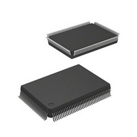
M30627FJPGP#D5C Renesas Electronics America, M30627FJPGP#D5C Datasheet - Page 210

M30627FJPGP#D5C
Manufacturer Part Number
M30627FJPGP#D5C
Description
MCU 3/5V 512K 128-LQFP
Manufacturer
Renesas Electronics America
Series
M16C™ M16C/60r
Datasheet
1.M30620SPGPU3C.pdf
(423 pages)
Specifications of M30627FJPGP#D5C
Core Processor
M16C/60
Core Size
16-Bit
Speed
24MHz
Connectivity
I²C, IEBus, UART/USART
Peripherals
DMA, WDT
Number Of I /o
111
Program Memory Size
512KB (512K x 8)
Program Memory Type
FLASH
Ram Size
31K x 8
Voltage - Supply (vcc/vdd)
2.7 V ~ 5.5 V
Data Converters
A/D 26x10b; D/A 2x8b
Oscillator Type
Internal
Operating Temperature
-20°C ~ 85°C
Package / Case
128-LQFP
Lead Free Status / RoHS Status
Contains lead / RoHS non-compliant
Eeprom Size
-
Available stocks
Company
Part Number
Manufacturer
Quantity
Price
Part Number:
M30627FJPGP#D5CM30627FJPGP#U3C
Manufacturer:
Renesas Electronics America
Quantity:
10 000
- Current page: 210 of 423
- Download datasheet (5Mb)
M16C/62P Group (M16C/62P, M16C/62PT)
Rev.2.41
REJ09B0185-0241
Figure 17.14
17.1.1.1
17.1.1.2
If a communication error occurs while transmitting or receiving in clock synchronous serial I/O mode, follow
the procedures below.
Use the CKPOL bit in the UiC0 register (i = 0 to 2) to select the transfer clock polarity. Figure 17.14 shows the
Transfer Clock Polarity.
(1) When the CKPOL bit in the UiC0 register = 0 (transmit data output at the falling
(2) When the CKPOL bit = 1 (transmit data output at the rising edge and the receive
CLKi
TXDi
RXDi
CLKi
TXDi
RXDi
•
(1) Set the RE bit in the UiC1 register to “0” (reception disabled)
(2) Set the SMD2 to SMD0 bits in the UiMR register to “000b” (Serial interface disabled)
(3) Set the SMD2 to SMD0 bits in the UiMR register to “001b” (Clock synchronous serial I/O mode)
(4) Set the RE bit in the UiC1 register to “1” (reception enabled)
•
(1) Set the SMD2 to SMD0 bits in the UiMR register “000b” (Serial interface disabled)
(2) Set the SMD2 to SMD0 bits in the UiMR register “001b” (Clock synchronous serial I/O mode)
(3) “1” is written to RE bit in the UiC1 register (transmission enabled), regardless of the TE bit in the UiCi
Jan 10, 2006
Resetting the UiRB register (i=0 to 2)
Resetting the UiTB register (i=0 to 2)
edge and the receive data taken in at the rising edge of the transfer clock)
data taken in at the falling edge of the transfer clock)
NOTES:
i = 0 to 2
register
1. This applies to the case where the UFORM bit in the UiC0 register = 0
2. When not transferring, the CLKi pin outputs a high signal.
3. When not transferring, the CLKi pin outputs a low signal.
Counter Measure for Communication Error Occurs
CLK Polarity Select Function
Transfer Clock Polarity
(LSB first) and the UiLCH bit in the UiC1 register = 0 (no reverse).
Page 193 of 390
D0
D0
D0
D0
D1
D1
D1
D1
D2
D2
D2
D2
D3
D3
D3
D3
D4
D4
D4
D4
D5
D5
D5
D5
D6
D6
D6
D6
D7
D7
D7
D7
17. Serial Interface
(NOTE 2)
(NOTE 3)
Related parts for M30627FJPGP#D5C
Image
Part Number
Description
Manufacturer
Datasheet
Request
R

Part Number:
Description:
KIT STARTER FOR M16C/29
Manufacturer:
Renesas Electronics America
Datasheet:

Part Number:
Description:
KIT STARTER FOR R8C/2D
Manufacturer:
Renesas Electronics America
Datasheet:

Part Number:
Description:
R0K33062P STARTER KIT
Manufacturer:
Renesas Electronics America
Datasheet:

Part Number:
Description:
KIT STARTER FOR R8C/23 E8A
Manufacturer:
Renesas Electronics America
Datasheet:

Part Number:
Description:
KIT STARTER FOR R8C/25
Manufacturer:
Renesas Electronics America
Datasheet:

Part Number:
Description:
KIT STARTER H8S2456 SHARPE DSPLY
Manufacturer:
Renesas Electronics America
Datasheet:

Part Number:
Description:
KIT STARTER FOR R8C38C
Manufacturer:
Renesas Electronics America
Datasheet:

Part Number:
Description:
KIT STARTER FOR R8C35C
Manufacturer:
Renesas Electronics America
Datasheet:

Part Number:
Description:
KIT STARTER FOR R8CL3AC+LCD APPS
Manufacturer:
Renesas Electronics America
Datasheet:

Part Number:
Description:
KIT STARTER FOR RX610
Manufacturer:
Renesas Electronics America
Datasheet:

Part Number:
Description:
KIT STARTER FOR R32C/118
Manufacturer:
Renesas Electronics America
Datasheet:

Part Number:
Description:
KIT DEV RSK-R8C/26-29
Manufacturer:
Renesas Electronics America
Datasheet:

Part Number:
Description:
KIT STARTER FOR SH7124
Manufacturer:
Renesas Electronics America
Datasheet:

Part Number:
Description:
KIT STARTER FOR H8SX/1622
Manufacturer:
Renesas Electronics America
Datasheet:

Part Number:
Description:
KIT DEV FOR SH7203
Manufacturer:
Renesas Electronics America
Datasheet:


