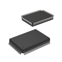
M30627FJPGP#D5C Renesas Electronics America, M30627FJPGP#D5C Datasheet - Page 418

M30627FJPGP#D5C
Manufacturer Part Number
M30627FJPGP#D5C
Description
MCU 3/5V 512K 128-LQFP
Manufacturer
Renesas Electronics America
Series
M16C™ M16C/60r
Datasheet
1.M30620SPGPU3C.pdf
(423 pages)
Specifications of M30627FJPGP#D5C
Core Processor
M16C/60
Core Size
16-Bit
Speed
24MHz
Connectivity
I²C, IEBus, UART/USART
Peripherals
DMA, WDT
Number Of I /o
111
Program Memory Size
512KB (512K x 8)
Program Memory Type
FLASH
Ram Size
31K x 8
Voltage - Supply (vcc/vdd)
2.7 V ~ 5.5 V
Data Converters
A/D 26x10b; D/A 2x8b
Oscillator Type
Internal
Operating Temperature
-20°C ~ 85°C
Package / Case
128-LQFP
Lead Free Status / RoHS Status
Contains lead / RoHS non-compliant
Eeprom Size
-
Available stocks
Company
Part Number
Manufacturer
Quantity
Price
Part Number:
M30627FJPGP#D5CM30627FJPGP#U3C
Manufacturer:
Renesas Electronics America
Quantity:
10 000
- Current page: 418 of 423
- Download datasheet (5Mb)
Rev.
REVISION HISTORY
Date
15-17 Tables 1.10 to 1.12 Pin Characteristics for 128-Pin Package are added.
18-19 Figure 1.7 and 1.8 Pin Configuration (Top View) are partly revised.
20-21 Tables 1.13 to 1.14 Pin Characteristics for 100-Pin Package are added.
23-24 Tables 1.15 to 1.16 Pin Characteristics for 80-Pin Package are added.
25-29 Tables 1.17 to 1.21 are partly revised.
40-44 Change sections in Chapter 5.
52-53 6.4 Cold Start-up / Warm Start-up Determine Function is added.
Page
100
104
107
118
119
120
14
22
34
42
45
48
49
57
64
69
80
89
90
91
94
95
96
97
98
99
Figure 1.6 Pin Configuration (Top View) is partly revised.
Figure 1.9 Pin Configuration (Top View) is partly revised.
Note 4 of Table 4.1 SFR Information is partly revised.
5.2 Brown-out Detection Reset (Hardware Reset 2) is partly revised.
6. Voltage Detection Circuit is partly revised.
Figure 6.1 Voltage Detection Circuit Block is partly revised.
Figure 6.4 Typical Operation of Brown-out Detection Reset (Hardware
Reset 2) is partly revised.
Table 6.2 Sampling Periods is partly revised.
Note 7 of Figure 7.2 PM1 Register is partly revised.
8.2.6 RDY Signal is partly revised.
Table 8.8 Bit and Bus Cycle Related to Software
Figure 9.8 Relationship Between Address on 4-Mbyte ROM and Those on
Microcomputer (2) is partly revised.
Figure 10.7 Examples of Main Clock Connection Circuit is partly revised.
Figure 10.8 Examples of Sub Clock Connection Circuit is partly revised.
10.1.4 PLL Clock is partly revised.
10.4.1.6 On-chip Oscillator Mode is partly revised.
10.4.1.7 On-chip Oscillator Low Power Dissipation Mode is partly revised.
Table 10.4 Pin Status During Wait Mode is partly revised.
10.4.2.4 Exiting Wait Mode is partly revised.
10.4.3 Stop Mode is partly revised.
Table 10.6 Interrupts to Stop Mode and Use Conditions is added.
10.4.3.3 Exiting Stop Mode is partly revised.
Figure 10.11 State Transition in Normal Operating Mode is partly revised.
10.6.3 How to Use Oscillation Stop and Re-oscillation Detect Function is
partly revised.
12.2.2 Overflow Interrupt is partly revised.
12.5.8 Returning from an Interrupt Routine is partly revised.
12.5.9 Interrupt Priority is partly revised.
12.5.10 Interrupt Priority Level Select Circuit is partly revised.
Figure 12.11 IFSR and IFSR2A Registers (Interrupt Factor Select
Register) is partly revised.
M16C/62P Group (M16C/62P, M16C/62PT) Hardware Manual
C - 11
Description
Summary
Related parts for M30627FJPGP#D5C
Image
Part Number
Description
Manufacturer
Datasheet
Request
R

Part Number:
Description:
KIT STARTER FOR M16C/29
Manufacturer:
Renesas Electronics America
Datasheet:

Part Number:
Description:
KIT STARTER FOR R8C/2D
Manufacturer:
Renesas Electronics America
Datasheet:

Part Number:
Description:
R0K33062P STARTER KIT
Manufacturer:
Renesas Electronics America
Datasheet:

Part Number:
Description:
KIT STARTER FOR R8C/23 E8A
Manufacturer:
Renesas Electronics America
Datasheet:

Part Number:
Description:
KIT STARTER FOR R8C/25
Manufacturer:
Renesas Electronics America
Datasheet:

Part Number:
Description:
KIT STARTER H8S2456 SHARPE DSPLY
Manufacturer:
Renesas Electronics America
Datasheet:

Part Number:
Description:
KIT STARTER FOR R8C38C
Manufacturer:
Renesas Electronics America
Datasheet:

Part Number:
Description:
KIT STARTER FOR R8C35C
Manufacturer:
Renesas Electronics America
Datasheet:

Part Number:
Description:
KIT STARTER FOR R8CL3AC+LCD APPS
Manufacturer:
Renesas Electronics America
Datasheet:

Part Number:
Description:
KIT STARTER FOR RX610
Manufacturer:
Renesas Electronics America
Datasheet:

Part Number:
Description:
KIT STARTER FOR R32C/118
Manufacturer:
Renesas Electronics America
Datasheet:

Part Number:
Description:
KIT DEV RSK-R8C/26-29
Manufacturer:
Renesas Electronics America
Datasheet:

Part Number:
Description:
KIT STARTER FOR SH7124
Manufacturer:
Renesas Electronics America
Datasheet:

Part Number:
Description:
KIT STARTER FOR H8SX/1622
Manufacturer:
Renesas Electronics America
Datasheet:

Part Number:
Description:
KIT DEV FOR SH7203
Manufacturer:
Renesas Electronics America
Datasheet:


