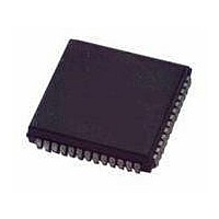
MC68711E20CFNE3 Freescale Semiconductor, MC68711E20CFNE3 Datasheet - Page 93

MC68711E20CFNE3
Manufacturer Part Number
MC68711E20CFNE3
Description
IC MCU 8BIT 52-PLCC
Manufacturer
Freescale Semiconductor
Series
HC11r
Datasheet
1.MC711D3CFNE2R.pdf
(138 pages)
Specifications of MC68711E20CFNE3
Core Processor
HC11
Core Size
8-Bit
Speed
3MHz
Connectivity
SCI, SPI
Peripherals
POR, WDT
Number Of I /o
38
Program Memory Size
20KB (20K x 8)
Program Memory Type
OTP
Eeprom Size
512 x 8
Ram Size
768 x 8
Voltage - Supply (vcc/vdd)
4.5 V ~ 5.5 V
Data Converters
A/D 8x8b
Oscillator Type
Internal
Operating Temperature
-40°C ~ 85°C
Package / Case
52-PLCC
Processor Series
M687xx
Core
HC11
Data Bus Width
8 bit
Data Ram Size
768 B
Interface Type
SCI, SPI
Maximum Clock Frequency
3 MHz
Number Of Programmable I/os
38
Number Of Timers
8
Maximum Operating Temperature
+ 85 C
Mounting Style
SMD/SMT
Minimum Operating Temperature
- 40 C
On-chip Adc
8 bit, 8 Channel
Lead Free Status / RoHS Status
Lead free / RoHS Compliant
Available stocks
Company
Part Number
Manufacturer
Quantity
Price
Company:
Part Number:
MC68711E20CFNE3
Manufacturer:
TI
Quantity:
101
Company:
Part Number:
MC68711E20CFNE3
Manufacturer:
Freescale Semiconductor
Quantity:
10 000
8.4.2 Timer Compare Force Register
The timer compare force register (CFORC) allows forced early compares. FOC1–FOC5 correspond to
the five output compares. These bits are set for each output compare that is to be forced. The action taken
as a result of a forced compare is the same as if there were a match between the OCx register and the
free-running counter, except that the corresponding interrupt status flag bits are not set. The forced
channels trigger their programmed pin actions to occur at the next timer count transition after the write to
CFORC.
The CFORC bits should not be used on an output compare function that is programmed to toggle its
output on a successful compare because a normal compare that occurs immediately before or after the
force can result in an undesirable operation.
FOC1–FOC5 — Write 1s to Force Compare Bits
Bits 2–0 — Not implemented, always read 0.
8.4.3 Output Compare 1 Mask Register
Use OC1M with OC1 to specify the bits of port A that are affected by a successful OC1 compare. The bits
of the OC1M register correspond to PA7–PA3.
OC1M7–OC1M3 — Output Compare Masks
Bits 2–0 — Not implemented; always read 0.
Freescale Semiconductor
Set bit(s) to enable OC1 to control corresponding pin(s) of port A.
0 = Not affected
1 = Output x action occurs
0 = OC1 disabled
1 = OC1 enabled to control the corresponding pin of port A
Address:
Address:
Reset:
Reset:
Read:
Read:
Write:
Write:
OC1M7
$000B
$000C
FOC1
Bit 7
Bit 7
Figure 8-8. Output Compare 1 Mask Register (OC1M)
0
0
Figure 8-7. Timer Compare Force Register (CFORC)
OC1M6
FOC2
6
0
6
0
MC68HC711D3 Data Sheet, Rev. 2.1
OC1M5
FOC3
5
0
5
0
OC1M4
FOC4
4
0
4
0
OC1M3
FOC5
3
0
3
0
2
0
0
2
0
0
1
0
0
1
0
0
Output Compare (OC)
Bit 0
Bit 0
0
0
0
0
93


