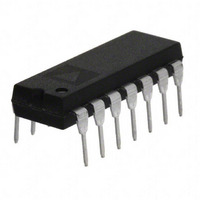
OP497GPZ Analog Devices Inc, OP497GPZ Datasheet

OP497GPZ
Specifications of OP497GPZ
Available stocks
Related parts for OP497GPZ
OP497GPZ Summary of contents
Page 1
FEATURES Low offset voltage: 75 μV maximum Low offset voltage drift: 1.0 μV/°C maximum Very low bias current 25°C: 150 pA maximum −40°C to +85°C: 300 pA maximum Very high open-loop gain: 2000 V/mV minimum Low supply current (per amplifier): ...
Page 2
OP497 TABLE OF CONTENTS Features .............................................................................................. 1 Applications ....................................................................................... 1 General Description ......................................................................... 1 Pin Connections ............................................................................... 1 Revision History ............................................................................... 2 Specifications ..................................................................................... 3 Absolute Maximum Ratings ............................................................ 4 Thermal Resistance ...................................................................... 4 ESD Caution .................................................................................. 4 Typical Performance ...
Page 3
SPECIFICATIONS T = 25° ±15 V, unless otherwise noted Table 1. Parameter Symbol INPUT CHARACTERISTICS Offset Voltage V Average Input Offset Voltage Drift TCV Long-Term Input Offset Voltage Stability Input Bias Current I Average Input Bias ...
Page 4
OP497 ABSOLUTE MAXIMUM RATINGS Absolute maximum ratings apply to packaged parts. Table 2. Parameter Supply Voltage 1 Input Voltage 1 Differential Input Voltage Output Short-Circuit Duration Storage Temperature Range Operating Temperature Range Junction Temperature Range Lead Temperature (Soldering, 60 sec) ...
Page 5
TYPICAL PERFORMANCE CHARACTERISTICS T = 25° ±15 V, unless otherwise noted –100 –80 –60 –40 – INPUT OFFSET VOLTAGE (µV) Figure 5. Typical Distribution of Input Offset Voltage ...
Page 6
OP497 ±3 ±2 ± TIME AFTER POWER APPLIED (Minutes) Figure 11. Input Offset Voltage Warm-Up Drift 10k BALANCED OR UNBALANCED V = ±15V 100 100 ...
Page 7
GAIN 60 PHASE –20 –40 100 1k 10k 100k FREQUENCY (Hz) Figure 17. Open-Loop Gain and Phase vs. Frequency 10k T = 25° 125° ±15V ...
Page 8
OP497 +V S –0.5 –1.0 –1.5 1.5 1.0 0.5 – ±5 ±10 SUPPLY VOLTAGE (V) Figure 23. Input Common-Mode Voltage Range vs. Supply Voltage ±15V 25° VCL ...
Page 9
V = ±15V 25° VCL V = 100mV p-p OUT 100 1k LOAD CAPACITANCE (pF) Figure 29. Small-Signal Overshoot vs. Load Capacitance 10k Rev. ...
Page 10
OP497 APPLICATIONS INFORMATION Extremely low bias current makes the OP497 attractive for use in sample-and-hold amplifiers, peak detectors, and log amplifiers that must operate over a wide temperature range. Balancing input resistances is not necessary with the OP497. High source ...
Page 11
GUARDING AND SHIELDING To maintain the extremely high input impedances of the OP497, care must be taken in circuit board layout and manufacturing. Board surfaces must be kept scrupulously clean and free of moisture. Conformal coating is recommended to provide ...
Page 12
OP497 APPLICATIONS CIRCUIT PRECISION ABSOLUTE VALUE AMPLIFIER The circuit in Figure precision absolute value amplifier with an input impedance of 30 MΩ. The high gain and low TCV of the OP497 ensure accurate operation with microvolt OS ...
Page 13
NONLINEAR CIRCUITS Due to its low input bias currents, the OP497 is an ideal log amplifier in nonlinear circuits, such as the squaring amplifier and square root amplifier circuits shown in Figure 40 and Figure 41. Using the squaring amplifier ...
Page 14
OP497 OUTLINE DIMENSIONS 0.210 (5.33) MAX 0.150 (3.81) 0.130 (3.30) 0.110 (2.79) 0.022 (0.56) 0.018 (0.46) 0.014 (0.36) 0.30 (0.0118) 0.10 (0.0039) COPLANARITY 0.10 0.775 (19.69) 0.750 (19.05) 0.735 (18.67 0.280 (7.11) 0.250 (6.35) 1 0.240 (6.10) 7 ...
Page 15
... Model Temperature Range OP497FP −40°C to +85°C 1 OP497FPZ −40°C to +85°C OP497GP −40°C to +85°C 1 OP497GPZ −40°C to +85°C OP497FS −40°C to +85°C OP497FS-REEL −40°C to +85°C 1 OP497FSZ −40°C to +85°C OP497FSZ-REEL −40°C to +85°C OP497GS − ...
Page 16
OP497 NOTES ©1991–2009 Analog Devices, Inc. All rights reserved. Trademarks and registered trademarks are the property of their respective owners. D00309-0-2/09(E) Rev Page ...


