OP497GPZ Analog Devices Inc, OP497GPZ Datasheet - Page 4
OP497GPZ
Manufacturer Part Number
OP497GPZ
Description
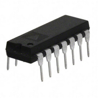
IC OPAMP GP 500KHZ QUAD 14DIP
Manufacturer
Analog Devices Inc
Datasheet
1.OP497GPZ.pdf
(16 pages)
Specifications of OP497GPZ
Slew Rate
0.15 V/µs
Amplifier Type
General Purpose
Number Of Circuits
4
Gain Bandwidth Product
500kHz
Current - Input Bias
60pA
Voltage - Input Offset
80µV
Current - Supply
525µA
Current - Output / Channel
25mA
Voltage - Supply, Single/dual (±)
±2 V ~ 20 V
Operating Temperature
-40°C ~ 85°C
Mounting Type
Through Hole
Package / Case
14-DIP (0.300", 7.62mm)
Op Amp Type
Precision
No. Of Amplifiers
4
Bandwidth
500kHz
Supply Voltage Range
± 2V To ± 20V
Amplifier Case Style
DIP
No. Of Pins
14
Lead Free Status / RoHS Status
Lead free / RoHS Compliant
Output Type
-
-3db Bandwidth
-
Lead Free Status / RoHS Status
Lead free / RoHS Compliant, Lead free / RoHS Compliant
Available stocks
Company
Part Number
Manufacturer
Quantity
Price


OP497
ABSOLUTE MAXIMUM RATINGS
Absolute maximum ratings apply to packaged parts.
Table 2.
Parameter
Supply Voltage
Input Voltage
Differential Input Voltage
Output Short-Circuit Duration
Storage Temperature Range
Operating Temperature Range
Junction Temperature Range
Lead Temperature (Soldering, 60 sec)
1
Stresses above those listed under Absolute Maximum Ratings
may cause permanent damage to the device. This is a stress
rating only; functional operation of the device at these or any
other conditions above those indicated in the operational
section of this specification is not implied. Exposure to absolute
maximum rating conditions for extended periods may affect
device reliability.
For supply voltages less than ±20 V, the absolute maximum input voltage is
equal to the supply voltage.
1
1
Rating
±20 V
20 V
40 V
Indefinite
−65°C to +150°C
−40°C to +85°C
−65°C to +150°C
300°C
Rev. E | Page 4 of 16
THERMAL RESISTANCE
θ
θ
θ
(PCB) for the SOIC package.
Table 3.
Package Type
14-Lead PDIP (N-14)
16-Lead SOIC (RW-16)
ESD CAUTION
CHANNEL SEPARATION = 20 log
JA
JA
JA
is specified for the worst-case mounting conditions, that is,
is specified for a device in socket for the PDIP package, and
is specified for a device soldered to the printed circuit board
–
OP497
+
1/4
Figure 4. Channel Separation Test Circuit
(
2kΩ
V
2
/10,000
V
V
1
1
50Ω
20V p-p @ 10Hz
θ
76
92
JA
)
–
OP497
+
50kΩ
1/4
θ
33
23
JC
Unit
°C/W
°C/W
V
2
Related parts for OP497GPZ
Image
Part Number
Description
Manufacturer
Datasheet
Request
R

Part Number:
Description:
±1.7g Dual-Axis IMEMS Accelerometer Evaluation Board
Manufacturer:
Analog Devices Inc
Datasheet:

Part Number:
Description:
Inertial Sensor Evaluation System
Manufacturer:
Analog Devices Inc
Datasheet:
Part Number:
Description:
Manufacturer:
Analog Devices Inc
Datasheet:
Part Number:
Description:
Manufacturer:
Analog Devices Inc
Datasheet:
Part Number:
Description:
Manufacturer:
Analog Devices Inc
Datasheet:
Part Number:
Description:
Manufacturer:
Analog Devices Inc
Datasheet:
Part Number:
Description:
Manufacturer:
Analog Devices Inc
Datasheet:
Part Number:
Description:
Manufacturer:
Analog Devices Inc
Datasheet:
Part Number:
Description:
Manufacturer:
Analog Devices Inc
Datasheet:
Part Number:
Description:
Manufacturer:
Analog Devices Inc
Datasheet:
Part Number:
Description:
Manufacturer:
Analog Devices Inc
Datasheet:
Part Number:
Description:
Manufacturer:
Analog Devices Inc
Datasheet:
Part Number:
Description:
Manufacturer:
Analog Devices Inc
Datasheet: