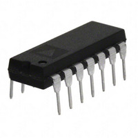
OP497GPZ Analog Devices Inc, OP497GPZ Datasheet - Page 13

OP497GPZ
Manufacturer Part Number
OP497GPZ
Description
IC OPAMP GP 500KHZ QUAD 14DIP
Manufacturer
Analog Devices Inc
Datasheet
1.OP497GPZ.pdf
(16 pages)
Specifications of OP497GPZ
Slew Rate
0.15 V/µs
Amplifier Type
General Purpose
Number Of Circuits
4
Gain Bandwidth Product
500kHz
Current - Input Bias
60pA
Voltage - Input Offset
80µV
Current - Supply
525µA
Current - Output / Channel
25mA
Voltage - Supply, Single/dual (±)
±2 V ~ 20 V
Operating Temperature
-40°C ~ 85°C
Mounting Type
Through Hole
Package / Case
14-DIP (0.300", 7.62mm)
Op Amp Type
Precision
No. Of Amplifiers
4
Bandwidth
500kHz
Supply Voltage Range
± 2V To ± 20V
Amplifier Case Style
DIP
No. Of Pins
14
Lead Free Status / RoHS Status
Lead free / RoHS Compliant
Output Type
-
-3db Bandwidth
-
Lead Free Status / RoHS Status
Lead free / RoHS Compliant, Lead free / RoHS Compliant
Available stocks
Company
Part Number
Manufacturer
Quantity
Price
NONLINEAR CIRCUITS
Due to its low input bias currents, the OP497 is an ideal log
amplifier in nonlinear circuits, such as the squaring amplifier
and square root amplifier circuits shown in Figure 40 and
Figure 41. Using the squaring amplifier circuit in Figure 40
as an example, the analysis begins by writing a voltage loop
equation across Transistors Q1, Q2, Q3, and Q4.
All the transistors in the
the same temperature; therefore, the I
giving
Exponentiating both sides of the thick equation lead to
Op amp A2 forms a current-to-voltage converter which results
in V
equation for I
V
IN
OUT
2InI
133kΩ
V
V
I
O
R1
T1
OUT
In
= R2 × I
=
IN
⎛
⎜
⎜
⎝
( )
= InI
=
I
I
I
I
IN
I
IN
REF
IN
S1
⎛
⎜
⎜
⎝
O
I
⎞
⎟
⎟
⎠
2
R2
yields
REF
O
+
O
2
3
. Substituting (V
+ InI
V
OP497
T2
⎞
⎟
⎟
⎠
A1
Figure 40. Squaring Amplifier
1/4
⎛
⎜
⎝
2
In
V
Q1
V+
V–
REF
R1
⎛
⎜
⎜
⎝
IN
4
8
1
I
3
I
MAT04
100pF
IN
S2
= In ( I
⎞
⎟
⎠
C1
1
2
⎞
⎟
⎟
⎠
6
=
Q2
V
O
7
5
T3
are precisely matched and at
10
IN
× I
In
8
Q3
/R1) for I
⎛
⎜
⎜
⎝
REF
I
O
I
S
9
50kΩ
I
I
and V
100pF
R3
)
6
MAT04
5
S3
O
C2
OP497
⎞
⎟
⎟
⎠
1/4
–15V
+
A2
IN
V
T
R4
50kΩ
T4
terms cancel,
I
and the previous
REF
33kΩ
In
R2
14
12
⎛
⎜
⎜
⎝
7
Q4
I
I
REF
S4
13
⎞
⎟
⎟
⎠
V
OUT
Rev. E | Page 13 of 16
A similar analysis made for the square root amplifier circuit in
Figure 41 leads to its transfer function
In these circuits, I
maintain accuracy, the negative supply should be well regulated.
For applications where very high accuracy is required, a voltage
reference can be used to set I
the squaring circuit is that a sufficiently large input voltage can
force the output beyond the operating range of the output op
amp. Resistor R4 can be changed to scale I
be varied to keep the output voltage within the usable range.
Unadjusted accuracy of the square root circuit is better than
0.1% over an input voltage range of 100 mV to 10 V. For a similar
input voltage range, the accuracy of the squaring circuit is better
than 0.5%.
V
IN
V
33kΩ
R1
OUT
=
R2
100pF
C1
2
3
REF
(
OP497
V
Figure 41. Square Root Amplifier
is a function of the negative power supply. To
1/4
IN
V+
V–
I
IN
R1
8
4
)(
I
REF
1
REF
)
. An important consideration for
2kΩ
R5
2
6
Q1
Q2
1
5
3
7
I
O
10
MAT04
8
33kΩ
6
5
Q3
R2
REF
OP497
50kΩ
R3
1/4
9
, or R1 and R2 can
13
100pF
–15V
C2
Q4
14
12
R4
50kΩ
7
I
REF
OP497
V
OUT


