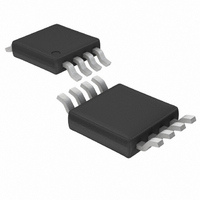
LT1819CMS8 Linear Technology, LT1819CMS8 Datasheet

LT1819CMS8
Specifications of LT1819CMS8
Available stocks
Related parts for LT1819CMS8
LT1819CMS8 Summary of contents
Page 1
... TSOT-23 and SO-8 packages; the LT1819 (dual op amp) is available in MSOP-8 and SO-8 packages. L, LT, LTC, LTM, Linear Technology and the Linear logo are registered trademarks of Linear Technology Corporation. ThinSOT is a trademark of Linear Technology Corporation. All other trademarks are the property of their respective owners. ...
Page 2
... LT1818CS5#TRPBF LT1818IS5#PBF LT1818IS5#TRPBF LT1818CS8#PBF LT1818CS8#TRPBF LT1818IS8#PBF LT1818IS8#TRPBF LT1819CMS8#PBF LT1819CMS8#TRPBF LT1819IMS8#PBF LT1819IMS8#TRPBF LT1819CS8#PBF LT1819CS8#TRPBF LT1819IS8#PBF LT1819IS8#TRPBF Consult LTC Marketing for parts specifi ed with wider operating temperature ranges. *The temperature grade is identifi label on the shipping container. Consult LTC Marketing for information on non-standard lead based fi nish parts. ...
Page 3
ELECTRICAL CHARACTERISTICS temperature range, otherwise specifi cations are at T SYMBOL PARAMETER V Input Offset Voltage OS /ΔT Input Offset Voltage Drift Δ Input Offset Current OS I Input Bias Current B e Input Noise Voltage Density n ...
Page 4
LT1818/LT1819 ELECTRICAL CHARACTERISTICS temperature range, otherwise specifi cations are at T SYMBOL PARAMETER GBW Gain-Bandwidth Product Rise Time, Fall Time Propagation Delay PD OS Overshoot t Settling Time S HD Harmonic Distortion dG Differential ...
Page 5
ELECTRICAL CHARACTERISTICS temperature range, otherwise specifi cations are at T SYMBOL PARAMETER A Large-Signal Voltage Gain VOL Channel Separation V Output Swing (Positive) OUT Output Swing (Negative) I Output Current OUT I Output Short-Circuit Current SC SR Slew Rate FPBW ...
Page 6
LT1818/LT1819 ELECTRICAL CHARACTERISTICS Note 5: With ±5V supplies, slew rate is tested in a closed-loop gain of –1 by measuring the rise time of the output from – with an output step from –3V to 3V. With single ...
Page 7
TYPICAL PERFORMANCE CHARACTERISTICS Open-Loop Gain vs Temperature ± ± 100Ω 500Ω –50 – 100 TEMPERATURE (°C) 18189 ...
Page 8
LT1818/LT1819 TYPICAL PERFORMANCE CHARACTERISTICS Gain vs Frequency 500Ω 100Ω 25°C A – ± 500Ω ...
Page 9
TYPICAL PERFORMANCE CHARACTERISTICS Distortion vs Frequency –60 2ND 100Ω L 3RD 100Ω L –70 –80 2ND 500Ω L –90 3RD 500Ω L –100 –110 ...
Page 10
LT1818/LT1819 APPLICATIONS INFORMATION Layout and Passive Components As with all high speed amplifi ers, the LT1818/LT1819 require some attention to board layout. A ground plane is recommended and trace lengths should be minimized, especially on the negative input lead. Low ...
Page 11
APPLICATIONS INFORMATION Slew Rate The slew rate of the LT1818/LT1819 is proportional to the differential input voltage. Highest slew rates are therefore seen in the lowest gain confi gurations. For example output step with a gain of 10 ...
Page 12
LT1818/LT1819 TYPICAL APPLICATION 10μ Single Supply Differential ADC Driver 5V 18pF + 51.1Ω 1/2 LT1819 – 18pF 536Ω 536Ω – 51.1Ω 1/2 LT1819 4.99k + 18pF 4.99k 0.1μF Results Obtained with the Circuit of Figure 2 ...
Page 13
SIMPLIFIED SCHEMATIC + V –IN – V (One Amplifi er) + LT1818/LT1819 OUT 18189 SS 18189fb 13 ...
Page 14
LT1818/LT1819 PACKAGE DESCRIPTION 5.23 (.206) MIN 0.42 0.038 (.0165 .0015) TYP RECOMMENDED SOLDER PAD LAYOUT 0.254 (.010) GAUGE PLANE 0.18 (.007) NOTE: 1. DIMENSIONS IN MILLIMETER/(INCH) 2. DRAWING NOT TO SCALE 3. DIMENSION DOES NOT INCLUDE MOLD FLASH, PROTRUSIONS OR ...
Page 15
PACKAGE DESCRIPTION 0.62 MAX 3.85 MAX 2.62 REF RECOMMENDED SOLDER PAD LAYOUT PER IPC CALCULATOR 0.20 BSC DATUM ‘A’ 0.30 – 0.50 REF NOTE: 1. DIMENSIONS ARE IN MILLIMETERS 2. DRAWING NOT TO SCALE 3. DIMENSIONS ARE INCLUSIVE OF PLATING ...
Page 16
LT1818/LT1819 PACKAGE DESCRIPTION .050 BSC .245 MIN .030 .005 TYP RECOMMENDED SOLDER PAD LAYOUT .010 – .020 (0.254 – 0.508) .008 – .010 (0.203 – 0.254) (0.406 – 1.270) NOTE: 1. DIMENSIONS IN 2. DRAWING NOT TO SCALE 3. THESE ...
Page 17
... Updated Order Information Section Information furnished by Linear Technology Corporation is believed to be accurate and reliable. However, no responsibility is assumed for its use. Linear Technology Corporation makes no representa- tion that the interconnection of its circuits as described herein will not infringe on existing patent rights. LT1818/LT1819 ...
Page 18
... Low Noise: 3.5nV/√Hz Low Distortion: –90dBc at 5MHz Low Power: 3.6mA Max at ±5V Programmable Supply Current 1.9nV/√Hz Noise, 3mA Max www.linear.com ● V OUT Large-Signal Transient Response 18189 TA07 10ns/DIV LT 0510 REV B • PRINTED IN USA © LINEAR TECHNOLOGY CORPORATION 2002 18189fb ...


