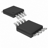
LT1819CMS8 Linear Technology, LT1819CMS8 Datasheet - Page 10

LT1819CMS8
Manufacturer Part Number
LT1819CMS8
Description
IC OPAMP 9MA 400MHZ DUAL 8MSOP
Manufacturer
Linear Technology
Datasheet
1.LT1819CS8PBF.pdf
(18 pages)
Specifications of LT1819CMS8
Amplifier Type
Voltage Feedback
Number Of Circuits
2
Slew Rate
2500 V/µs
Gain Bandwidth Product
400MHz
Current - Input Bias
2µA
Voltage - Input Offset
200µV
Current - Supply
9mA
Current - Output / Channel
70mA
Voltage - Supply, Single/dual (±)
2.5 V ~ 12.6 V, ±1.25 V ~ 6.3 V
Operating Temperature
0°C ~ 70°C
Mounting Type
Surface Mount
Package / Case
8-MSOP, Micro8™, 8-uMAX, 8-uSOP,
Lead Free Status / RoHS Status
Contains lead / RoHS non-compliant
Output Type
-
-3db Bandwidth
-
Available stocks
Company
Part Number
Manufacturer
Quantity
Price
Company:
Part Number:
LT1819CMS8
Manufacturer:
LT
Quantity:
10 000
Part Number:
LT1819CMS8
Manufacturer:
LINEAR/凌特
Quantity:
20 000
Part Number:
LT1819CMS8#PBF
Manufacturer:
LINEAR/凌特
Quantity:
20 000
Part Number:
LT1819CMS8#TRPBF
Manufacturer:
LINEAR/凌特
Quantity:
20 000
LT1818/LT1819
APPLICATIONS INFORMATION
Layout and Passive Components
As with all high speed amplifi ers, the LT1818/LT1819
require some attention to board layout. A ground plane
is recommended and trace lengths should be minimized,
especially on the negative input lead.
Low ESL/ESR bypass capacitors should be placed directly
at the positive and negative supply (0.01μF ceramics are
recommended). For high drive current applications, ad-
ditional 1μF to 10μF tantalums should be added.
The parallel combination of the feedback resistor and gain
setting resistor on the inverting input combine with the
input capacitance to form a pole that can cause peaking or
even oscillations. If feedback resistors greater than 500Ω
are used, a parallel capacitor of value
should be used to cancel the input pole and optimize
dynamic performance (see Figure 1). For applications
where the DC noise gain is 1 and a large feedback resis-
tor is used, C
example would be an I-to-V converter.
In high closed-loop gain confi gurations, R
needs to be added. To optimize the bandwidth in these
applications, a capacitor, C
R
Capacitive Loading
The LT1818/LT1819 are optimized for low distortion and
high gain bandwidth applications. The amplifi ers can drive
a capacitive load of 20pF in a unity-gain confi guration and
more with higher gain. When driving a larger capacitive
10
G
C
in order to cancel out any parasitic C
F
> R
G
• C
F
IN
should be greater than or equal to C
/R
F
G
, may be added in parallel with
IN
IN
F
+
–
capacitance.
F
>> R
R
C
G
G
G
, no C
IN
. An
+
–
Figure 1
F
R
C
F
F
load, a resistor of 10Ω to 50Ω must be connected between
the output and the capacitive load to avoid ringing or
oscillation (see R
taken directly from the output so that the series resistor
will isolate the capacitive load to ensure stability.
Input Considerations
The inputs of the LT1818/LT1819 amplifi ers are connected
to the bases of NPN and PNP bipolar transistors in paral-
lel. The base currents are of opposite polarity and provide
fi rst order bias current cancellation. Due to variation in the
matching of NPN and PNP beta, the polarity of the input
bias current can be positive or negative. The offset current,
however, does not depend on beta matching and is tightly
controlled. Therefore, the use of balanced source resistance
at each input is recommended for applications where DC
accuracy must be maximized. For example, with a 100Ω
source resistance at each input, the 800nA maximum offset
current results in only 80μV of extra offset, while without
balance the 8μA maximum input bias current could result
in an 0.8mV offset condition.
The inputs can withstand differential input voltages of
up to 6V without damage and without needing clamping
or series resistance for protection. This differential input
voltage generates a large internal current (up to 50mA),
which results in the high slew rate. In normal transient
closed-loop operation, this does not increase power dis-
sipation signifi cantly because of the low duty cycle of the
transient inputs. Sustained differential inputs, however,
will result in excessive power dissipation and therefore
this device should not be used as a comparator.
18189 F01
R
S
C
LOAD
S
in Figure 1). The feedback must still be
18189fb


