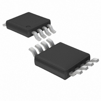
LT1819CMS8 Linear Technology, LT1819CMS8 Datasheet - Page 5

LT1819CMS8
Manufacturer Part Number
LT1819CMS8
Description
IC OPAMP 9MA 400MHZ DUAL 8MSOP
Manufacturer
Linear Technology
Datasheet
1.LT1819CS8PBF.pdf
(18 pages)
Specifications of LT1819CMS8
Amplifier Type
Voltage Feedback
Number Of Circuits
2
Slew Rate
2500 V/µs
Gain Bandwidth Product
400MHz
Current - Input Bias
2µA
Voltage - Input Offset
200µV
Current - Supply
9mA
Current - Output / Channel
70mA
Voltage - Supply, Single/dual (±)
2.5 V ~ 12.6 V, ±1.25 V ~ 6.3 V
Operating Temperature
0°C ~ 70°C
Mounting Type
Surface Mount
Package / Case
8-MSOP, Micro8™, 8-uMAX, 8-uSOP,
Lead Free Status / RoHS Status
Contains lead / RoHS non-compliant
Output Type
-
-3db Bandwidth
-
Available stocks
Company
Part Number
Manufacturer
Quantity
Price
Company:
Part Number:
LT1819CMS8
Manufacturer:
LT
Quantity:
10 000
Part Number:
LT1819CMS8
Manufacturer:
LINEAR/凌特
Quantity:
20 000
Part Number:
LT1819CMS8#PBF
Manufacturer:
LINEAR/凌特
Quantity:
20 000
Part Number:
LT1819CMS8#TRPBF
Manufacturer:
LINEAR/凌特
Quantity:
20 000
ELECTRICAL CHARACTERISTICS
SYMBOL
A
V
I
I
SR
FPBW
GBW
t
t
OS
HD
dG
dP
I
Note 1: Stresses beyond those listed under Absolute Maximum Ratings
may cause permanent damage to the device. Exposure to any Absolute
Maximum Rating condition for extended periods may affect device
reliability and lifetime.
Note 2: Differential inputs of ±6V are appropriate for transient operation
only, such as during slewing. Large sustained differential inputs can cause
excessive power dissipation and may damage the part.
temperature range, otherwise specifi cations are at T
OUT
SC
r
PD
S
VOL
OUT
, t
f
PARAMETER
Large-Signal Voltage Gain
Channel Separation
Output Swing (Positive)
Output Swing (Negative)
Output Current
Output Short-Circuit Current
Slew Rate
Full-Power Bandwidth
Gain-Bandwidth Product
Rise Time, Fall Time
Propagation Delay
Overshoot
Harmonic Distortion
Differential Gain
Differential Phase
Supply Current
CONDITIONS
V
V
V
R
R
R
R
V
V
A
A
2V
f = 4MHz, R
A
A
A
HD2, A
HD3, A
A
A
Per Amplifi er
V
V
V
V
V
V
V
OUT
OUT
OUT
OUT
OUT
L
L
L
L
T
T
T
T
T
T
T
T
T
T
T
T
T
T
T
T
T
T
T
T
T
T
T
T
P-P
A
A
A
A
A
A
A
A
A
A
A
A
A
A
A
A
A
A
= 1
= –1 (Note 5)
A
A
A
A
= 1, 10% to 90%, 0.1V Step
= 1, 50% to 50%, 0.1V Step
= 1, 0.1V, R
= 2, R
= 2, R
A
A
= 500Ω, 30mV Overdrive
= 100Ω, 30mV Overdrive
= 500Ω, 30mV Overdrive
= 100Ω, 30mV Overdrive
= 0°C to 70°C
= –40°C to 85°C
= 0°C to 70°C
= –40°C to 85°C
= 0°C to 70°C
= –40°C to 85°C
= 0°C to 70°C
= –40°C to 85°C
= 0°C to 70°C
= –40°C to 85°C
= 0°C to 70°C
= –40°C to 85°C
= 0°C to 70°C
= –40°C to 85°C
= 0°C to 70°C
= –40°C to 85°C
= 0°C to 70°C
= –40°C to 85°C
= 0°C to 70°C
= –40°C to 85°C
= 0°C to 70°C
= –40°C to 85°C
= 0°C to 70°C
= –40°C to 85°C
= 1.5V to 3.5V, R
= 1.5V to 3.5V, R
= 1.5V to 3.5V, LT1819
= 1.5V or 3.5V, 30mV Overdrive
= 2.5V, 1V Overdrive (Note 3)
(Note 6)
V
V
A
= 2, f = 5MHz, V
= 2, f = 5MHz, V
L
L
= 25°C. (Note 9) V
= 150Ω
= 150Ω
L
= 500Ω
L
The
= 100Ω
l
L
L
denotes the specifi cations which apply over the full operating
= 500Ω
= 100Ω
OUT
OUT
Note 3: A heat sink may be required to keep the junction temperature
below absolute maximum when the output is shorted indefi nitely.
Note 4: Input offset voltage is pulse tested and is exclusive of warm-up
drift.
= 2V
= 2V
S
= 5V, 0V; V
P-P
P-P
, R
, R
L
L
= 500Ω
= 500Ω
CM
= 2.5V, R
l
l
l
l
l
l
l
l
l
l
l
l
l
l
l
l
l
l
l
l
l
l
L
MIN
±30
±25
±20
±80
±70
±50
450
375
300
240
230
220
1.0
0.7
0.6
0.7
0.5
0.4
3.9
3.8
3.7
3.7
3.6
3.5
to 2.5V unless otherwise noted.
81
80
79
LT1818/LT1819
±140
1000
0.07
0.07
TYP
100
±50
800
125
360
–72
–74
4.2
0.8
0.7
1.1
8.5
20
2
4
4
1
MAX
1.1
1.2
1.3
1.3
1.4
1.5
10
13
14
UNITS
18189fb
V/mV
V/mV
V/mV
V/mV
V/mV
V/mV
5
V/μs
V/μs
V/μs
V/μs
MHz
MHz
MHz
MHz
DEG
dBc
dBc
mA
mA
mA
mA
mA
mA
mA
mA
mA
dB
dB
dB
ns
ns
%
%
V
V
V
V
V
V
V
V
V
V
V
V


