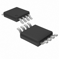
LT1819CMS8 Linear Technology, LT1819CMS8 Datasheet - Page 6

LT1819CMS8
Manufacturer Part Number
LT1819CMS8
Description
IC OPAMP 9MA 400MHZ DUAL 8MSOP
Manufacturer
Linear Technology
Datasheet
1.LT1819CS8PBF.pdf
(18 pages)
Specifications of LT1819CMS8
Amplifier Type
Voltage Feedback
Number Of Circuits
2
Slew Rate
2500 V/µs
Gain Bandwidth Product
400MHz
Current - Input Bias
2µA
Voltage - Input Offset
200µV
Current - Supply
9mA
Current - Output / Channel
70mA
Voltage - Supply, Single/dual (±)
2.5 V ~ 12.6 V, ±1.25 V ~ 6.3 V
Operating Temperature
0°C ~ 70°C
Mounting Type
Surface Mount
Package / Case
8-MSOP, Micro8™, 8-uMAX, 8-uSOP,
Lead Free Status / RoHS Status
Contains lead / RoHS non-compliant
Output Type
-
-3db Bandwidth
-
Available stocks
Company
Part Number
Manufacturer
Quantity
Price
Company:
Part Number:
LT1819CMS8
Manufacturer:
LT
Quantity:
10 000
Part Number:
LT1819CMS8
Manufacturer:
LINEAR/凌特
Quantity:
20 000
Part Number:
LT1819CMS8#PBF
Manufacturer:
LINEAR/凌特
Quantity:
20 000
Part Number:
LT1819CMS8#TRPBF
Manufacturer:
LINEAR/凌特
Quantity:
20 000
LT1818/LT1819
ELECTRICAL CHARACTERISTICS
Note 5: With ±5V supplies, slew rate is tested in a closed-loop gain of –1
by measuring the rise time of the output from –2V to 2V with an output
step from –3V to 3V. With single 5V supplies, slew rate is tested in a
closed-loop gain of –1 by measuring the rise time of the output from 1.5V
to 3.5V with an output step from 1V to 4V. Falling edge slew rate is not
production tested, but is designed, characterized and expected to be within
10% of the rising edge slew rate.
Note 6: Full-power bandwidth is calculated from the slew rate:
Note 7: This parameter is not 100% tested.
TYPICAL PERFORMANCE CHARACTERISTICS
6
FPBW = SR/2πV
–0.4
–0.8
–1.2
–1.6
–2.0
–2.4
–2.8
12
10
6
0
8
4
2
0
–50
–50 –25
Supply Current vs Temperature
Input Bias Current vs Temperature
V
PER AMPLIFIER
CM
–25
= 0V
V
V
0
0
TEMPERATURE (°C)
P
S
S
TEMPERATURE (°C)
= ±5V
= ±2.5V
25
25
V
V
S
S
= ±2.5V
50
= ±5V
50
75
75
100
100
18189 G01
18189 G04
125
125
100
10
1
–0.5
–1.0
–1.5
–2.0
10
2.0
1.5
1.0
0.5
V
V
Input Noise Spectral Density
+
–
0
Input Common Mode Range
vs Supply Current
T
A
V
= 25°C
OS
1
100
< 1mV
FREQUENCY (Hz)
SUPPLY VOLTAGE (±V)
2
1k
3
e
i
n
n
Note 8: The LT1818C/LT1818I and LT1819C/LT1819I are guaranteed
functional over the operating temperature range of –40°C to 85°C.
Note 9: The LT1818C/LT1819C are guaranteed to meet specifi ed
performance from 0°C to 70°C and is designed, characterized and
expected to meet the extended temperature limits, but is not tested
at –40°C and 85°C. The LT1818I/LT1819I are guaranteed to meet the
extended temperature limits.
Note 10: Thermal resistance (θ
metal connected to the package. The specifi ed values are for short
traces connected to the leads. If desired, the thermal resistance can be
signifi cantly reduced by connecting the V
4
10k
T
V
A
R
5
A
S
V
S
= 25°C
= ±5V
= 101
= 10k
18189 G05
6
18189 G02
100k
1
10
0.1
7
–2
–4
–6
–8
80
77
74
71
68
65
62
JA
2
0
–5
100
) varies with the amount of PC board
Input Bias Current vs Common
Mode Voltage
Open-Loop Gain vs Resistive Load
T
V
T
A
S
A
= 25°C
= ±5V
= 25°C
INPUT COMMON MODE VOLTAGE (V)
–
–2.5
pin to a large metal area.
LOAD RESISTANCE (Ω)
1k
0
V
V
S
S
= ±5V
= ±2.5V
2.5
18189 G03
18189 G06
18189fb
10k
5


