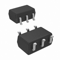
LMH6601QMGX/NOPB National Semiconductor, LMH6601QMGX/NOPB Datasheet - Page 20

LMH6601QMGX/NOPB
Manufacturer Part Number
LMH6601QMGX/NOPB
Description
IC AMP VFA 2.4V SHUTDOWN SC70-6
Manufacturer
National Semiconductor
Datasheet
1.LMH6601MGNOPB.pdf
(28 pages)
Specifications of LMH6601QMGX/NOPB
Amplifier Type
Voltage Feedback
Number Of Circuits
1
Output Type
Rail-to-Rail
Slew Rate
275 V/µs
Gain Bandwidth Product
155MHz
-3db Bandwidth
250MHz
Current - Input Bias
5pA
Voltage - Input Offset
1000µV
Current - Supply
9.6mA
Current - Output / Channel
180mA
Voltage - Supply, Single/dual (±)
2.4 V ~ 5.5 V, ±1.2 V ~ 2.75 V
Operating Temperature
-40°C ~ 85°C
Mounting Type
Surface Mount
Package / Case
SC-70-6, SC-88, SOT-363
Number Of Channels
1
Voltage Gain Db
66 dB
Common Mode Rejection Ratio (min)
56 dB
Input Offset Voltage
2.4 mV at 5 V
Operating Supply Voltage
3 V, 5 V
Supply Current
11.5 mA at 5 V
Maximum Operating Temperature
+ 85 C
Minimum Operating Temperature
- 40 C
Lead Free Status / RoHS Status
Lead free / RoHS Compliant
Other names
LMH6601QMGX
www.national.com
The final set of values for R
which will result in the proper gain and correct video levels
(0V to 1V) at the output (V
AC COUPLED VIDEO
Many monitors and displays accept AC coupled inputs. This
simplifies the amplification and buffering task in some re-
spects. As can be seen in
input to the center of the input linear range while C
ples the video onto the op amp’s input. The op amp is set for
a closed loop gain of 2 with R
sure the device output is also biased at mid-supply. Because
SAG COMPENSATION
The capacitors shown in
C
costly and take up valuable real estate on the board. It is pos-
sible to reduce the value of the output coupling capacitor,
C
compensation. SAG refers to what the output video experi-
ences due to the low frequency video content it contains
O
O
, are the large electrolytic type which are considerably
, which is the largest of all, by using what is called SAG
Estimate
R
820
620
390
560
G
1k
(Ω)
Figure 8
(from
LOAD
Figure
Calculated
G
TABLE 1. Finding
F
R3 (Ω)
and R
Equation
1.30k
).
1.69k
1.56k
1.37k
239
and R
(except C
8, R
3
1
G
in Table 1 are values
and R
. C
FIGURE 8. AC Coupled Video Amplifier/Driver
2)
G
G2
is there to make
), and especially
2
simply set the
Figure 7
IN
AC cou-
Equation 1
Calculated
External Resistor Values by Iteration
0.988
1.15
1.45
4.18
1.59
20
LHS
of the DC bias at the output, the load needs to be AC coupled
as well through C
valued ceramic capacitor (not shown) in parallel with C
which is electrolytic. The reason for this is that the ceramic
capacitor will tend to shunt the inductive behavior of the Elec-
trolytic capacitor at higher frequencies for an improved overall
low impedance output.
C
improve the video frequency response. This value is to be set
and trimmed on the board to meet the application’s specific
system requirements.
which cannot adequately go through the output AC coupling
scheme due to the low frequency limit of this circuit. The −3
dB low frequency limit of the output circuit is given by:
A possible implementation of the SAG compensation is
shown in
G2
f_low_frequency (−3 dB)= 1/ (2*pi* 75*2(Ω) * C
is intended to boost the high frequency gain in order to
Figure
(Compare
Increase
Increase
Increase
Reduce
Close to target value of 1.5V/V for
=
∼
9.
4.82 Hz For C
O
Equation 1
. Some applications implement a small
Equation 1
Equation 1
Equation 1
Equation 1
Comment
O
LHS by increasing R
LHS by reducing R
LHS by reducing R
LHS by reducing R
20136449
= 220 μF
LHS Calculated to RHS)
Equation 1
O
G
G
G
)
G
(3)
O


