LMH6601QMGX/NOPB National Semiconductor, LMH6601QMGX/NOPB Datasheet - Page 7

LMH6601QMGX/NOPB
Manufacturer Part Number
LMH6601QMGX/NOPB
Description
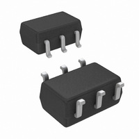
IC AMP VFA 2.4V SHUTDOWN SC70-6
Manufacturer
National Semiconductor
Datasheet
1.LMH6601MGNOPB.pdf
(28 pages)
Specifications of LMH6601QMGX/NOPB
Amplifier Type
Voltage Feedback
Number Of Circuits
1
Output Type
Rail-to-Rail
Slew Rate
275 V/µs
Gain Bandwidth Product
155MHz
-3db Bandwidth
250MHz
Current - Input Bias
5pA
Voltage - Input Offset
1000µV
Current - Supply
9.6mA
Current - Output / Channel
180mA
Voltage - Supply, Single/dual (±)
2.4 V ~ 5.5 V, ±1.2 V ~ 2.75 V
Operating Temperature
-40°C ~ 85°C
Mounting Type
Surface Mount
Package / Case
SC-70-6, SC-88, SOT-363
Number Of Channels
1
Voltage Gain Db
66 dB
Common Mode Rejection Ratio (min)
56 dB
Input Offset Voltage
2.4 mV at 5 V
Operating Supply Voltage
3 V, 5 V
Supply Current
11.5 mA at 5 V
Maximum Operating Temperature
+ 85 C
Minimum Operating Temperature
- 40 C
Lead Free Status / RoHS Status
Lead free / RoHS Compliant
Other names
LMH6601QMGX
I
VOH1
VOH2
VOH3
VOL1
VOL2
VOL3
I
I
Load
R
R
C
Miscellaneous Performance
VDMAX
VDMIN
I
V
T
T
Isolation
CC
O
O
i
on
off
_glitch
O
O
O
_1
Note 1: Absolute Maximum Ratings indicate limits beyond which damage to the device may occur. Operating Ratings indicate conditions for which the device is
intended to be functional, but specific performance is not guaranteed. For guaranteed specifications and the test conditions, see the Electrical Characteristics.
Note 2: Electrical Table values apply only for factory testing conditions at the temperature indicated. Factory testing conditions result in very limited self-heating
of the device such that T
T
Note 3: The maximum continuous output current (I
Note 4: Human Body Model, applicable std. MIL-STD-883, Method 3015.7. Machine Model, applicable std. JESD22-A115-A (ESD MM std. of JEDEC)
Field-Induced Charge-Device Model, applicable std. JESD22-C101-C (ESD FICDM std. of JEDEC).
Note 5: SD logic is CMOS compatible. To ensure proper logic level and to minimize power supply current, SD should typically be less than 10% of total supply
voltage away from either supply rail.
Note 6: Typical values represent the most likely parametric norm as determined at the time of characterization. Actual typical values may vary over time and will
also depend on the application and configuration. The typical values are not tested and are not guaranteed on shipped production material.
Note 7: Negative input current implies current flowing out of the device.
Note 8: Drift determined by dividing the change in parameter at temperature extremes by the total temperature change.
Note 9: This parameter is guaranteed by design and/or characterization and is not tested in production.
Note 10: “V
Symbol
_Enable
_Disabled Output Resistance
_Disabled Output Capacitance
A
.
OFF
ID
” is input differential voltage (input overdrive).
Supply Current
Output High Voltage
(Relative to V
Output Low Voltage
(Relative to V
Output Current
Output Load Rating
Output Resistance
Voltage Limit for Disable (Pin 5)
Voltage Limit for Enable (Pin 5)
Logic Input Current (Pin 5)
Turn-on Glitch
Turn-on Time
Turn-off Time
Off Isolation
J
= T
A
Parameter
. No guarantee of parametric performance is indicated in the electrical tables under conditions of internal self-heating where T
+
–
)
)
OUT
) is determined by device power dissipation limitations.
Normal Operation
V
Shutdown
SD tied to
R
R
R
R
R
R
V
Supply
V
(Note
THD < −30 dBc, f = 200 kHz, R
V
Enabled, A
Shutdown
Shutdown
(Note
(Note
SD = 2.7V
1 MHz, R
OUT
OUT
OUT
S
L
L
L
L
L
L
/2, V
= 150Ω to V
= 75Ω to V
= 10 kΩ to V
= 150Ω to V
= 75Ω to V
= 10 kΩ to V
≤
= V
= V
10)
5)
5)
OUT
0.6V from Respective
S
S
L
/2
/2, V
≤
(Note
= 1 kΩ
V
= 2.2 V
0.27V
= +1
S
S
Condition
ID
/2
/2
–
–
–
–
7
= ±18 mV
5)
PP
(Note
5)
Source
Sink
Source
Sink
L
tied to
(Note
–260
–420
2.43
Min
–50
100
25
35
0
6)
(Note
–200
–200
+125
>100
Typ
100
–10
760
9.0
0.2
5.6
1.2
5.2
+4
+4
25
62
40
60
4
6)
(Note
+125
10.6
12.5
0.27
Max
+45
+45
125
2.7
www.national.com
6)
Units
mA
mV
mV
mA
MΩ
nA
pA
dB
pF
µs
ns
Ω
Ω
V
V
V
J
>


