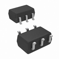
LMH6601QMGX/NOPB National Semiconductor, LMH6601QMGX/NOPB Datasheet - Page 21

LMH6601QMGX/NOPB
Manufacturer Part Number
LMH6601QMGX/NOPB
Description
IC AMP VFA 2.4V SHUTDOWN SC70-6
Manufacturer
National Semiconductor
Datasheet
1.LMH6601MGNOPB.pdf
(28 pages)
Specifications of LMH6601QMGX/NOPB
Amplifier Type
Voltage Feedback
Number Of Circuits
1
Output Type
Rail-to-Rail
Slew Rate
275 V/µs
Gain Bandwidth Product
155MHz
-3db Bandwidth
250MHz
Current - Input Bias
5pA
Voltage - Input Offset
1000µV
Current - Supply
9.6mA
Current - Output / Channel
180mA
Voltage - Supply, Single/dual (±)
2.4 V ~ 5.5 V, ±1.2 V ~ 2.75 V
Operating Temperature
-40°C ~ 85°C
Mounting Type
Surface Mount
Package / Case
SC-70-6, SC-88, SOT-363
Number Of Channels
1
Voltage Gain Db
66 dB
Common Mode Rejection Ratio (min)
56 dB
Input Offset Voltage
2.4 mV at 5 V
Operating Supply Voltage
3 V, 5 V
Supply Current
11.5 mA at 5 V
Maximum Operating Temperature
+ 85 C
Minimum Operating Temperature
- 40 C
Lead Free Status / RoHS Status
Lead free / RoHS Compliant
Other names
LMH6601QMGX
In this circuit, the output coupling capacitor value and size is
reduced at the expense of a slightly more complicated cir-
cuitry. Note that C1 is not only part of the SAG compensation,
but it also sets the amplifier’s DC gain to 0 dB so that the
output is set to mid-rail for linearity purposes. Also note that
exceptionally high values are chosen for the R1 and R2 bi-
asing resistors (510 kΩ). The LMH6601 has extremely low
input bias current which allows this selection thereby reducing
the C
polar capacitors which will reduce cost.
At high enough frequencies where both C
considered to be shorted out, R
loop gain is determined by:
At intermediate frequencies, where the C
periences low frequency gain loss, the R
vides feedback from the load side of C
gain reduced at these lower frequencies, the feedback to the
op amp inverting node reduces, causing an increase at the
op amp's output as a response.
For NTSC video, low values of C
black level shift occurs during the vertical blanking interval
(
C
output SAG. An especially tough pattern is the NTSC pattern
called “Pulse & Bar.” With this pattern the entire top and bot-
tom portion of the field is black level video where, for about
∼
Closed_loop_Gain (V/V)= V
O
1.5 ms) which has no video activity and thus is sensitive to
's charge dissipation through the load which could cause
IN
value in this circuit such that C
[R
L
/(R
L
+R
O
FIGURE 9. AC Coupled Video Amplifier/Driver with SAG Compensation
)]= 0.99V/V
L
/V
IN
3
O
= (1+ (R
shunts R
influence how much video
IN
O
. With the load side
can even be a non-
3
O
3
, R
, R
O
||R
4
and C
and the closed
5
O
4
, C
)/ R
, R
1
L
5
path pro-
1
)x
path ex-
can be
(4)
21
11 ms, C
tivity to replenish that charge.
Figure 10
the SAG.
With the circuit of
amplifier, the waveform duty cycle variations exert additional
restrictions on voltage swing at any node. This is illustrated in
the waveforms shown in
FIGURE 10.
O
shows the output of the
is discharging through the load with no video ac-
Figure 9
Figure 9
Scope Photo Showing Video SAG
Figure
and any other AC coupled pulse
11.
20136450
Figure 9
circuit highlighting
www.national.com
20136451


