LPC660IMX/NOPB National Semiconductor, LPC660IMX/NOPB Datasheet - Page 2
LPC660IMX/NOPB
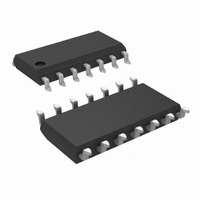
Manufacturer Part Number
LPC660IMX/NOPB
Description
IC OP AMP QUAD LOPWR CMOS 14SOIC
Manufacturer
National Semiconductor
Datasheet
1.LPC660AIMNOPB.pdf
(17 pages)
Specifications of LPC660IMX/NOPB
Amplifier Type
General Purpose
Number Of Circuits
4
Output Type
Rail-to-Rail
Slew Rate
0.11 V/µs
Gain Bandwidth Product
350kHz
Current - Input Bias
0.002pA
Voltage - Input Offset
1000µV
Current - Supply
160µA
Current - Output / Channel
40mA
Voltage - Supply, Single/dual (±)
4.75 V ~ 15.5 V, ±2.38 V ~ 7.75 V
Operating Temperature
-40°C ~ 85°C
Mounting Type
Surface Mount
Package / Case
14-SOIC (3.9mm Width), 14-SOL
Number Of Channels
4
Voltage Gain Db
120 dB
Common Mode Rejection Ratio (min)
63 dB
Input Offset Voltage
6 mV at 5 V
Operating Supply Voltage
9 V, 12 V
Supply Current
0.24 mA at 5 V
Maximum Operating Temperature
+ 85 C
Maximum Dual Supply Voltage
+/- 7.5 V
Minimum Operating Temperature
- 40 C
Lead Free Status / RoHS Status
Lead free / RoHS Compliant
-3db Bandwidth
-
Lead Free Status / Rohs Status
Details
Other names
*LPC660IMX
*LPC660IMX/NOPB
LPC660IMX
*LPC660IMX/NOPB
LPC660IMX


www.national.com
Input Offset Voltage
Input Offset Voltage
Average Drift
Input Bias Current
Input Offset Current
Input Resistance
Common Mode
Rejection Ratio
Positive Power Supply
Rejection Ratio
Negative Power Supply
Rejection Ratio
Input Common Mode
Voltage Range
Large Signal
Absolute Maximum Ratings
If Military/Aerospace specified devices are required,
please contact the National Semiconductor Sales Office/
Distributors for availability and specifications.
DC Electrical Characteristics
Unless otherwise specified, all limits guaranteed for T
= 0V, V
Differential Input Voltage
Supply Voltage (V
Output Short Circuit to V
Output Short Circuit to V
Lead Temperature
Storage Temp. Range
Junction Temperature (Note 2)
ESD Rating
Power Dissipation
Current at Input Pin
Current at Output Pin
Voltage at Input/Output Pin
(Soldering, 10 sec.)
(C = 100 pF, R = 1.5 kΩ)
Parameter
CM
= 1.5V, V
+
− V
O
= 2.5V, and R
−
)
+
−
0V ≤ V
V
5V ≤ V
0V ≤ V
V
For CMRR
R
+
+
L
= 15V
= 5V & 15V
= 100 kΩ (Note 5)
CM
+
−
Conditions
≤ 15V
≤ −10V
≤ 12.0V
L
>
>
(V
50 dB
1M unless otherwise specified.
−65˚C to +150˚C
±
+
) + 0.3V, (V
Supply Voltage
(Note 3)
(Note 11)
(Note 1)
(Note 2)
±
±
18 mA
1000V
260˚C
150˚C
5 mA
J
0.3V
16V
−
= 25˚C. Boldface limits apply at the temperature extremes. V
) −
V
0.002
0.001
+
1000
−0.4
Typ
1.3
>
83
83
94
− 1.9
1
2
1
Operating Ratings
Current at Power Supply Pin
Temperature Range
Supply Range
Power Dissipation
Thermal Resistance (θ
LPC660AM
LPC660AI
LPC660I
14-Pin Ceramic DIP
14-Pin Molded DIP
14-Pin SO
14-Pin Side Brazed Ceramic DIP
LPC660AMJ/883
LPC660AM
(Notes 4, 8)
V
V
Limit
+
+
−0.1
100
100
400
3.5
20
20
70
68
70
68
84
82
− 2.3
− 2.6
3
0
JA
LPC660AI
(Note 4)
V
V
), (Note 10)
+
+
Limit
−0.1
400
3.3
70
68
70
68
84
83
− 2.3
− 2.5
3
4
2
0
(Note 3)
−40˚C ≤ T
−40˚C ≤ T
LPC660I
(Note 4)
V
V
Limit
+
+
−0.1
300
6.3
63
61
63
61
74
73
− 2.3
− 2.5
6
4
2
0
4.75V to 15.5V
−55˚C ≤ T
J
J
115˚C/W
+
(Note 9)
≤ +85˚C
≤ +85˚C
90˚C/W
85˚C/W
90˚C/W
+125˚C
= 5V, V
35 mA
Tera Ω
Units
µV/˚C
V/mV
max
max
max
max
min
min
min
min
mV
pA
pA
dB
dB
dB
V
V
J
≤
−
Related parts for LPC660IMX/NOPB
Image
Part Number
Description
Manufacturer
Datasheet
Request
R

Part Number:
Description:
Low Power Cmos Quad Operational Amplifier
Manufacturer:
National Semiconductor Corporation
Datasheet:

Part Number:
Description:
Manufacturer:
National Semiconductor
Datasheet:

Part Number:
Description:
IC OP AMP QUAD LP CMOS 14-SOIC
Manufacturer:
National Semiconductor
Datasheet:
Part Number:
Description:
LPC660 - Low Power CMOS Quad Operational Amplifier, Package: Soic Narrow, Pin Nb=14
Manufacturer:
National Semiconductor Corporation
Datasheet:
Part Number:
Description:
National Semiconductor [8-Bit D/A Converter]
Manufacturer:
National Semiconductor
Datasheet:
Part Number:
Description:
National Semiconductor [Media Coprocessor]
Manufacturer:
National Semiconductor
Datasheet:
Part Number:
Description:
Digitally Controlled Tone and Volume Circuit with Stereo Audio Power Amplifier, Microphone Preamp Stage and National 3D Sound
Manufacturer:
National Semiconductor
Datasheet:
Part Number:
Description:
Digitally Controlled Tone and Volume Circuit with Stereo Audio Power Amplifier, Microphone Preamp Stage and National 3D Sound
Manufacturer:
National Semiconductor
Datasheet:
Part Number:
Description:
AC97 Rev 2 Codec with Sample Rate Conversion and National 3D Sound
Manufacturer:
National Semiconductor
Part Number:
Description:
Manufacturer:
National Semiconductor
Datasheet:
Part Number:
Description:
Manufacturer:
National Semiconductor
Datasheet:
Part Number:
Description:
General Purpose, Low Voltage, Low Power, Rail-to-Rail Output Operational Amplifiers
Manufacturer:
National Semiconductor
Datasheet:
Part Number:
Description:
8-bit 20 MSPS flash A/D converter.
Manufacturer:
National Semiconductor
Datasheet:
Part Number:
Description:
Low Noise Quad Operational Amplifier
Manufacturer:
National Semiconductor
Datasheet: