LPC660IMX/NOPB National Semiconductor, LPC660IMX/NOPB Datasheet
LPC660IMX/NOPB
Specifications of LPC660IMX/NOPB
*LPC660IMX/NOPB
LPC660IMX


Related parts for LPC660IMX/NOPB


LPC660IMX/NOPB Summary of contents
Page 1
... Applications n High-impedance buffer n Precision current-to-voltage converter Application Circuit Oscillator frequency is determined by R1, R2, C1, and C2: where and C2. © 2004 National Semiconductor Corporation n Long-term integrator n High-impedance preamplifier n Active filter n Sample-and-Hold circuit n Peak detector Features n Rail-to-rail output swing n Micropower operation: n Specified for 100 kΩ ...
Page 2
... Absolute Maximum Ratings If Military/Aerospace specified devices are required, please contact the National Semiconductor Sales Office/ Distributors for availability and specifications. Differential Input Voltage + − Supply Voltage (V − Output Short Circuit to V − Output Short Circuit to V Lead Temperature (Soldering, 10 sec.) Storage Temp. Range ...
Page 3
DC Electrical Characteristics Unless otherwise specified, all limits guaranteed for 1.5V 2.5V, and Parameter Conditions Voltage Gain Sourcing Sinking kΩ (Note 5) L Sourcing Sinking + Output ...
Page 4
AC Electrical Characteristics Unless otherwise specified, all limits guaranteed for 1.5V 2.5, and Parameter Slew Rate (Note 6) Gain-Bandwidth Product Phase Margin Gain Margin Amp-to-Amp Isolation (Note 7) Input ...
Page 5
Typical Performance Characteristics ± 7.5V 25˚C unless otherwise specified S A Supply Current vs. Supply Voltage Common-Mode Voltage Range vs. Temperature Output Characteristics Current Sourcing Input Bias Current vs. Temperature 01054727 Output Characteristics Current Sinking 01054729 ...
Page 6
Typical Performance Characteristics Crosstalk Rejection vs. Frequency CMRR vs. Temperature Open-Loop Voltage Gain vs. Temperature www.national.com ± 7.5V 25˚C unless otherwise specified (Continued CMRR vs. Frequency 01054733 Power Supply Rejection Ratio vs. Frequency 01054735 ...
Page 7
Typical Performance Characteristics Gain and Phase Responses vs. Load Capacitance Gain Error (V vs Inverting Slew Rate vs. Temperature ± 7.5V Gain and Phase Responses vs. Temperature 01054739 ) Non-Inverting Slew Rate vs. ...
Page 8
Typical Performance Characteristics Non-Inverting Small Signal Pulse Response (A = +1) V Inverting Small-Signal Pulse Response Stability vs. Capacitive Load www.national.com ± 7.5V 25˚C unless otherwise specified (Continued Inverting Large-Signal Pulse Response 01054745 Stability ...
Page 9
Application Hints AMPLIFIER TOPOLOGY The topology chosen for the LPC660 is unconventional (compared to general-purpose op amps) in that the tradi- tional unity-gain buffer output stage is not used; instead, the output is taken directly from the output of the ...
Page 10
Application Hints (Continued) normally considered a very large resistance, could leak the trace were a 5V bus adjacent to the pad of an input. This would cause a 100 times degradation from the LPC660’s actual performance. However, ...
Page 11
Application Hints (Continued) The designer should be aware that when it is inappropriate to lay out a PC board for the sake of just a few circuits, there is another technique which is even better than a guard ring on ...
Page 12
Application Hints (Continued) (Input pins are lifted out of PC board and soldered directly to components. All other pins connected to PC board.) FIGURE 6. Air Wiring BIAS CURRENT TESTING The test method of Figure 7 is appropriate for bench-testing ...
Page 13
Typical Single-Supply Applications For good CMRR over temperature, low drift resistors should be used. Matching and affects CMRR. Gain may be adjusted through R2. CMRR may be adjusted through R7 ...
Page 14
Typical Single-Supply Applications ( 5 (Continued) DC Sine-Wave Oscillator Oscillator frequency is determined by R1, R2, C1, and C2 1/2πRC OSC where and C2. This ...
Page 15
Typical Single-Supply Applications ( 5 (Continued High-Pass Filter (2 dB Dip 0.895 Gain = Low-Pass Filter (Maximally Flat, Dual Supply Only) High Gain ...
Page 16
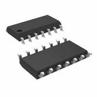
Connection Diagram Ordering Information Package 14-PinSOIC www.national.com 14-Pin DIP/SO Top View Part Number Transport Media LPC660AIM 55 Units/Rail LPC660AIMX 2.5k Tape and Reel LPC660IM 55 Units/Rail LPC660IMX 2.5k Tape and Reel 16 01054701 NSC Drawing M14A ...
Page 17
... BANNED SUBSTANCE COMPLIANCE National Semiconductor certifies that the products and packing materials meet the provisions of the Customer Products Stewardship Specification (CSP-9-111C2) and the Banned Substances and Materials of Interest Specification (CSP-9-111S2) and contain no ‘‘Banned Substances’’ as defined in CSP-9-111S2. ...