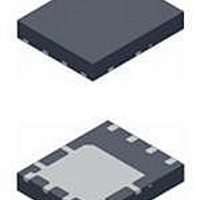
FDMS2510SDC Fairchild Semiconductor, FDMS2510SDC Datasheet - Page 2

FDMS2510SDC
Manufacturer Part Number
FDMS2510SDC
Description
MOSFET N-CH 20V DUAL POWER56
Manufacturer
Fairchild Semiconductor
Series
Dual Cool™, PowerTrench®, SyncFET™r
Datasheet
1.FDMS2510SDC.pdf
(9 pages)
Specifications of FDMS2510SDC
Fet Type
MOSFET N-Channel, Metal Oxide
Fet Feature
Logic Level Gate
Rds On (max) @ Id, Vgs
2.9 mOhm @ 23A, 10V
Drain To Source Voltage (vdss)
25V
Current - Continuous Drain (id) @ 25° C
28A
Vgs(th) (max) @ Id
3V @ 1mA
Gate Charge (qg) @ Vgs
45nC @ 10V
Input Capacitance (ciss) @ Vds
2780pF @ 13V
Power - Max
3.3W
Mounting Type
Surface Mount
Package / Case
*
Configuration
Dual
Transistor Polarity
N-Channel
Resistance Drain-source Rds (on)
2.9 mOhms
Forward Transconductance Gfs (max / Min)
159 S
Drain-source Breakdown Voltage
25 V
Gate-source Breakdown Voltage
20 V
Continuous Drain Current
49 A
Power Dissipation
60 W
Maximum Operating Temperature
+ 150 C
Mounting Style
SMD/SMT
Gate Charge Qg
15 nC
Minimum Operating Temperature
- 55 C
Lead Free Status / RoHS Status
Lead free / RoHS Compliant
Other names
FDMS2510SDCTR
Available stocks
Company
Part Number
Manufacturer
Quantity
Price
Company:
Part Number:
FDMS2510SDC
Manufacturer:
Fairchild Semiconductor
Quantity:
135
©2010 Fairchild Semiconductor Corporation
FDMS2510SDC Rev.C1
Electrical Characteristics
Off Characteristics
On Characteristics
Dynamic Characteristics
Switching Characteristics
Drain-Source Diode Characteristics
BV
ΔBV
I
I
V
r
g
C
C
C
R
t
t
t
t
Q
Q
Q
Q
V
t
Q
DSS
GSS
ΔV
d(on)
r
d(off)
f
rr
DS(on)
FS
GS(th)
SD
iss
oss
rss
g
ΔT
ΔT
g
g
gs
gd
rr
Symbol
DSS
GS(th)
DSS
J
J
Drain to Source Breakdown Voltage
Breakdown Voltage Temperature
Coefficient
Zero Gate Voltage Drain Current
Gate to Source Leakage Current, Forward
Gate to Source Threshold Voltage
Gate to Source Threshold Voltage
Temperature Coefficient
Static Drain to Source On Resistance
Forward Transconductance
Input Capacitance
Output Capacitance
Reverse Transfer Capacitance
Gate Resistance
Turn-On Delay Time
Rise Time
Turn-Off Delay Time
Fall Time
Total Gate Charge
Total Gate Charge
Gate to Source Gate Charge
Gate to Drain “Miller” Charge
Source to Drain Diode Forward Voltage
Reverse Recovery Time
Reverse Recovery Charge
Parameter
T
J
= 25 °C unless otherwise noted
V
V
V
V
V
f = 1 MHz
V
I
V
V
V
V
V
V
I
I
I
V
V
D
F
D
D
DD
GS
GS
GS
DS
GS
GS
GS
GS
DS
GS
GS
DS
GS
= 23 A, di/dt = 300 A/ μs
= 10 mA, referenced to 25 °C
= 1 mA, V
= 10 mA, referenced to 25 °C
= 13 V, V
= 13 V, I
= 10 V, R
= 0 V to 10 V
= 0 V to 4.5 V
= 5 V, I
= 0 V, I
= 0 V, I
= 20 V, V
= V
= 10 V, I
= 4.5 V, I
= 10 V, I
= 20 V, V
2
DS
Test Conditions
, I
D
S
S
D
GS
D
D
D
= 2 A
= 23 A
D
= 23 A
GS
GEN
GS
DS
= 1 mA
= 23 A,
= 23 A, T
= 23 A
= 18 A
= 0 V
= 0 V,
= 0 V
= 0 V
= 6 Ω
V
I
D
DD
= 23 A
J
= 13 V,
= 125 °C
(Note 2)
(Note 2)
Min
1.2
25
2090
0.48
0.79
577
128
159
1.1
Typ
1.7
2.4
3.4
3.5
6.3
4.0
23
17
10
27
32
15
-5
19
4
3
2780
Max
770
195
2.4
0.8
1.2
500
100
3.0
2.9
4.2
4.3
36
31
20
10
43
10
45
21
www.fairchildsemi.com
mV/°C
mV/°C
Units
mΩ
nC
pF
pF
pF
μA
nA
nC
nC
nC
nC
ns
Ω
ns
ns
ns
ns
V
S
V
V


