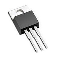
STP5N62K3 STMicroelectronics, STP5N62K3 Datasheet - Page 4

STP5N62K3
Manufacturer Part Number
STP5N62K3
Description
MOSFET N-CH 620V 4.2A TO220AB
Manufacturer
STMicroelectronics
Series
SuperMESH3™r
Datasheet
1.STP5N62K3.pdf
(19 pages)
Specifications of STP5N62K3
Fet Type
MOSFET N-Channel, Metal Oxide
Fet Feature
Standard
Rds On (max) @ Id, Vgs
1.6 Ohm @ 2.1A, 10V
Drain To Source Voltage (vdss)
620V
Current - Continuous Drain (id) @ 25° C
4.2A
Vgs(th) (max) @ Id
4.5V @ 50µA
Gate Charge (qg) @ Vgs
26nC @ 10V
Input Capacitance (ciss) @ Vds
680pF @ 50V
Power - Max
70W
Mounting Type
Through Hole
Package / Case
TO-220-3
Configuration
Single
Transistor Polarity
N-Channel
Resistance Drain-source Rds (on)
1.6 Ohms
Drain-source Breakdown Voltage
620 V
Power Dissipation
70 W
Maximum Operating Temperature
+ 150 C
Mounting Style
Through Hole
Gate Charge Qg
26 nC
Lead Free Status / RoHS Status
Lead free / RoHS Compliant
Other names
497-10771-5
Available stocks
Company
Part Number
Manufacturer
Quantity
Price
Company:
Part Number:
STP5N62K3
Manufacturer:
STMicroelectronics
Quantity:
500
Electrical characteristics
2
4/19
Electrical characteristics
(Tcase =25 °C unless otherwise specified)
Table 4.
Table 5.
1. C
C
V
Symbol
Symbol
R
OSS eq
V
(BR)DSS
increases from 0 to 80% V
C
I
I
C
DS(on)
C
GS(th)
Q
Q
DSS
GSS
Q
R
oss eq
oss
rss
iss
gs
gd
g
g
(1)
. is defined as a constant equivalent capacitance giving the same charging time as C
Input capacitance
Output capacitance
Reverse transfer
capacitance
Equivalent output
capacitance
Gate input resistance
Total gate charge
Gate-source charge
Gate-drain charge
Drain-source
breakdown voltage
Zero gate voltage
drain current (V
Gate-body leakage
current (V
Gate threshold voltage V
Static drain-source on
resistance
On /off states
Dynamic
Parameter
Parameter
DS
= 0)
DSS
GS
= 0)
Doc ID 17361 Rev 2
V
V
V
f=1 MHz open drain
V
V
(see Figure 20)
I
V
V
V
V
D
DS
GS
GS
DD
GS
GS
GS
DS
DS
DS
= 1 mA, V
= Max rating
= Max rating, T
= 50 V, f = 1 MHz,
= 0
= 0, V
= 10 V
= ± 20 V; V
= V
= 10 V, I
= 496 V, I
Test conditions
Test conditions
GS
DS
, I
GS
D
D
= 0 to 496 V
D
= 50 µA
= 2.1 A
= 0
DS
= 4.2 A,
=0
C
=125 °C
Min.
Min.
620
3
-
-
-
STB/D/F/P/U5N62K3
Typ.
Typ.
16.6
3.75
1.28
680
50
26
16
8
4
4
oss
when V
Max.
Max.
±10
4.5
1.6
50
1
-
-
-
D
Unit
Unit
S
µA
µA
µA
nC
nC
nC
pF
pF
pF
pF
V
V
Ω
Ω


