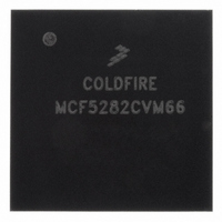
MCF5282CVM66 Freescale Semiconductor, MCF5282CVM66 Datasheet - Page 671

MCF5282CVM66
Manufacturer Part Number
MCF5282CVM66
Description
IC MPU 512K 66MHZ 256-MAPBGA
Manufacturer
Freescale Semiconductor
Series
MCF528xr
Datasheet
1.MCF5216CVM66J.pdf
(766 pages)
Specifications of MCF5282CVM66
Core Processor
Coldfire V2
Core Size
32-Bit
Speed
66MHz
Connectivity
CAN, EBI/EMI, Ethernet, I²C, SPI, UART/USART
Peripherals
DMA, LVD, POR, PWM, WDT
Number Of I /o
150
Program Memory Size
512KB (512K x 8)
Program Memory Type
FLASH
Ram Size
64K x 8
Voltage - Supply (vcc/vdd)
2.7 V ~ 3.6 V
Data Converters
A/D 8x10b
Oscillator Type
External
Operating Temperature
-40°C ~ 85°C
Package / Case
256-MAPBGA
Controller Family/series
ColdFire
No. Of I/o's
150
Ram Memory Size
64KB
Cpu Speed
66.67MHz
Embedded Interface Type
CAN, I2C, SPI, UART
No. Of Pwm Channels
8
Rohs Compliant
Yes
Lead Free Status / RoHS Status
Lead free / RoHS Compliant
Eeprom Size
-
Available stocks
Company
Part Number
Manufacturer
Quantity
Price
Company:
Part Number:
MCF5282CVM66
Manufacturer:
FREESCAL
Quantity:
152
Company:
Part Number:
MCF5282CVM66
Manufacturer:
Freescale Semiconductor
Quantity:
10 000
Part Number:
MCF5282CVM66
Manufacturer:
NXP/恩智浦
Quantity:
20 000
Company:
Part Number:
MCF5282CVM66J
Manufacturer:
Freescale Semiconductor
Quantity:
10 000
- Current page: 671 of 766
- Download datasheet (9Mb)
31.5.3.1 External Test Instruction (EXTEST)
The EXTEST instruction selects the boundary scan register. It forces all output pins and bidirectional pins
configured as outputs to the values preloaded with the SAMPLE/PRELOAD instruction and held in the
boundary scan update registers. EXTEST can also configure the direction of bidirectional pins and
establish high-impedance states on some pins. EXTEST asserts internal reset for the MCU system logic to
force a predictable internal state while performing external boundary scan operations.
31.5.3.2 IDCODE Instruction
The IDCODE instruction selects the 32-bit IDCODE register for connection as a shift path between the
TDI and TDO pin. This instruction allows interrogation of the MCU to determine its version number and
other part identification data. The shift register LSB is forced to logic 1 on the rising edge of TCLK
following entry into the capture-DR state.Therefore, the first bit to be shifted out after selecting the
IDCODE register is always a logic 1. The remaining 31 bits are also forced to fixed values on the rising
edge of TCLK following entry into the capture-DR state.
IDCODE is the default instruction placed into the instruction register when the TAP resets. Thus, after a
TAP reset, the IDCODE register is selected automatically.
31.5.3.3 SAMPLE/PRELOAD Instruction
The SAMPLE/PRELOAD instruction has two functions:
Freescale Semiconductor
LOCKOUT_RECOVERY
1
2
3
ENABLE_TEST_CTRL
Instruction for manufacturing purposes only
TRST pin assertion or power-on reset is required to exit this instruction.
Freescale reserves the right to change the decoding of the unused opcodes in the future.
SAMPLE/PRELOAD
TEST_LEAKAGE
•
Instruction
Reserved
SAMPLE - obtain a sample of the system data and control signals present at the MCU input pins
and just before the boundary scan cell at the output pins. This sampling occurs on the rising edge
of TCLK in the capture-DR state when the IR contains the $2 opcode. The sampled data is
EXTEST
IDCODE
BYPASS
CLAMP
HIGHZ
1,2
all others
MCF5282 and MCF5216 ColdFire Microcontroller User’s Manual, Rev. 3
IR[3:0]
0000
0010
1011
1111
0001
0101
0110
1001
1100
Selects boundary scan register while applying fixed values to output pins and
asserting functional reset
Selects IDCODE register for shift
Selects boundary scan register for shifting, sampling, and preloading without
disturbing functional operation
Selects bypass register while tri-stating all output pins and assert to high the
jtag_leakage signal
Selects TEST_CTRL register
Selects bypass register while tri-stating all output pins and asserting functional reset
Allows for the erase of the TFM flash when the part is secure
Selects bypass while applying fixed values to output pins and asserting functional
reset
Selects bypass register for data operations
Decoded to select bypass register
Table 31-5. JTAG Instructions
Instruction Summary
3
IEEE 1149.1 Test Access Port (JTAG)
31-7
Related parts for MCF5282CVM66
Image
Part Number
Description
Manufacturer
Datasheet
Request
R
Part Number:
Description:
Mcf5282 And Mcf5216 Coldfire Microcontroller User�s Manual
Manufacturer:
Freescale Semiconductor, Inc
Datasheet:
Part Number:
Description:
Manufacturer:
Freescale Semiconductor, Inc
Datasheet:
Part Number:
Description:
Manufacturer:
Freescale Semiconductor, Inc
Datasheet:
Part Number:
Description:
Manufacturer:
Freescale Semiconductor, Inc
Datasheet:
Part Number:
Description:
Manufacturer:
Freescale Semiconductor, Inc
Datasheet:
Part Number:
Description:
Manufacturer:
Freescale Semiconductor, Inc
Datasheet:
Part Number:
Description:
Manufacturer:
Freescale Semiconductor, Inc
Datasheet:
Part Number:
Description:
Manufacturer:
Freescale Semiconductor, Inc
Datasheet:
Part Number:
Description:
Manufacturer:
Freescale Semiconductor, Inc
Datasheet:
Part Number:
Description:
Manufacturer:
Freescale Semiconductor, Inc
Datasheet:
Part Number:
Description:
Manufacturer:
Freescale Semiconductor, Inc
Datasheet:
Part Number:
Description:
Manufacturer:
Freescale Semiconductor, Inc
Datasheet:
Part Number:
Description:
Manufacturer:
Freescale Semiconductor, Inc
Datasheet:
Part Number:
Description:
Manufacturer:
Freescale Semiconductor, Inc
Datasheet:
Part Number:
Description:
Manufacturer:
Freescale Semiconductor, Inc
Datasheet:


