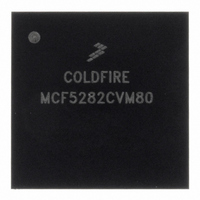
MCF5282CVM80 Freescale Semiconductor, MCF5282CVM80 Datasheet - Page 228

MCF5282CVM80
Manufacturer Part Number
MCF5282CVM80
Description
IC MPU 512K 80MHZ 256-MAPBGA
Manufacturer
Freescale Semiconductor
Series
MCF528xr
Datasheet
1.MCF5216CVM66J.pdf
(766 pages)
Specifications of MCF5282CVM80
Core Processor
Coldfire V2
Core Size
32-Bit
Speed
80MHz
Connectivity
CAN, EBI/EMI, Ethernet, I²C, SPI, UART/USART
Peripherals
DMA, LVD, POR, PWM, WDT
Number Of I /o
150
Program Memory Size
512KB (512K x 8)
Program Memory Type
FLASH
Ram Size
64K x 8
Voltage - Supply (vcc/vdd)
2.7 V ~ 3.6 V
Data Converters
A/D 8x10b
Oscillator Type
External
Operating Temperature
-40°C ~ 85°C
Package / Case
256-MAPBGA
Controller Family/series
ColdFire
Ram Memory Size
64KB
Embedded Interface Type
CAN, I2C, SPI, UART
No. Of Pwm Channels
8
Digital Ic Case Style
MAPBGA
Rohs Compliant
Yes
Lead Free Status / RoHS Status
Lead free / RoHS Compliant
Eeprom Size
-
Available stocks
Company
Part Number
Manufacturer
Quantity
Price
Company:
Part Number:
MCF5282CVM80
Manufacturer:
FREESCALE
Quantity:
1 831
Company:
Part Number:
MCF5282CVM80
Manufacturer:
Freescale Semiconductor
Quantity:
10 000
Company:
Part Number:
MCF5282CVM80J
Manufacturer:
Freescale Semiconductor
Quantity:
10 000
- Current page: 228 of 766
- Download datasheet (9Mb)
External Interface Module (EIM)
Basic operation of the bus is a three-clock bus cycle:
13.4.2
The data transfer operation is controlled by an on-chip state machine. Each bus clock cycle is divided into
two states. Even states occur when CLKOUT is high and odd states occur when CLKOUT is low. The state
transition diagram for basic and fast termination read and write cycles are shown in
13-4
1. During the first clock, the address, attributes, and TS are driven.
2. Data and TA are sampled during the second clock of a bus-read cycle. During a read, the external
3. The last clock of the bus cycle uses what would be an idle clock between cycles to provide hold
device provides data and is sampled at the rising edge at the end of the second bus clock. This data
is concurrent with TA, which is also sampled at the rising edge of the clock.
During a write, the ColdFire device drives data from the rising clock edge at the end of the first
clock to the rising clock edge at the end of the bus cycle. Wait states can be added between the first
and second clocks by delaying the assertion of TA. TA can be configured to be generated internally
through the CSCRs. If TA is not generated internally, the system must provide it externally.
time for address, attributes and write data.
write operations.
0
1
Multiple
0
1
Multiple
0
1
Multiple
Data Transfer Cycle States
Number of CSCR Matches
MCF5282 and MCF5216 ColdFire Microcontroller User’s Manual, Rev. 3
Table 13-2. Accesses by Matches in CSCRs and DACRs
0
1
Multiple
0
0
1
1
Multiple
Multiple
Number of DACR Matches
Figure 13-6
and
External
Defined by CSCR
External, burst-inhibited, 32-bit
Defined by DACRs
Undefined
Undefined
Undefined
Undefined
Undefined
Figure 13-8
Type of Access
show the basic read and
Freescale Semiconductor
Figure
13-4.
Related parts for MCF5282CVM80
Image
Part Number
Description
Manufacturer
Datasheet
Request
R
Part Number:
Description:
Mcf5282 And Mcf5216 Coldfire Microcontroller User�s Manual
Manufacturer:
Freescale Semiconductor, Inc
Datasheet:
Part Number:
Description:
Manufacturer:
Freescale Semiconductor, Inc
Datasheet:
Part Number:
Description:
Manufacturer:
Freescale Semiconductor, Inc
Datasheet:
Part Number:
Description:
Manufacturer:
Freescale Semiconductor, Inc
Datasheet:
Part Number:
Description:
Manufacturer:
Freescale Semiconductor, Inc
Datasheet:
Part Number:
Description:
Manufacturer:
Freescale Semiconductor, Inc
Datasheet:
Part Number:
Description:
Manufacturer:
Freescale Semiconductor, Inc
Datasheet:
Part Number:
Description:
Manufacturer:
Freescale Semiconductor, Inc
Datasheet:
Part Number:
Description:
Manufacturer:
Freescale Semiconductor, Inc
Datasheet:
Part Number:
Description:
Manufacturer:
Freescale Semiconductor, Inc
Datasheet:
Part Number:
Description:
Manufacturer:
Freescale Semiconductor, Inc
Datasheet:
Part Number:
Description:
Manufacturer:
Freescale Semiconductor, Inc
Datasheet:
Part Number:
Description:
Manufacturer:
Freescale Semiconductor, Inc
Datasheet:
Part Number:
Description:
Manufacturer:
Freescale Semiconductor, Inc
Datasheet:
Part Number:
Description:
Manufacturer:
Freescale Semiconductor, Inc
Datasheet:


