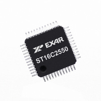
ST16C2550CQ48-F Exar Corporation, ST16C2550CQ48-F Datasheet - Page 4

ST16C2550CQ48-F
Manufacturer Part Number
ST16C2550CQ48-F
Description
IC DUART FIFO 16B 48TQFP
Manufacturer
Exar Corporation
Type
RS- 232 or RS- 485r
Datasheet
1.ST16C2550CJ44-F.pdf
(37 pages)
Specifications of ST16C2550CQ48-F
Number Of Channels
2, DUART
Package / Case
48-TQFP
Features
*
Fifo's
16 Byte
Protocol
RS232, RS485
Voltage - Supply
2.97 V ~ 5.5 V
With False Start Bit Detection
Yes
With Modem Control
Yes
With Cmos
Yes
Mounting Type
Surface Mount
Data Rate
4 Mbps
Supply Voltage (max)
5.5 V
Supply Voltage (min)
2.97 V
Supply Current
3 mA
Maximum Operating Temperature
+ 70 C
Minimum Operating Temperature
0 C
Mounting Style
SMD/SMT
Operating Supply Voltage
3.3 V or 5 V
No. Of Channels
2
Supply Voltage Range
2.97V To 5.5V
Operating Temperature Range
0°C To +70°C
Digital Ic Case Style
TQFP
No. Of Pins
48
Filter Terminals
SMD
Rohs Compliant
Yes
Lead Free Status / RoHS Status
Lead free / RoHS Compliant
Lead Free Status / RoHS Status
Lead free / RoHS Compliant, Lead free / RoHS Compliant
Other names
1016-1255
Available stocks
Company
Part Number
Manufacturer
Quantity
Price
Company:
Part Number:
ST16C2550CQ48-F
Manufacturer:
EXAR
Quantity:
4 800
Company:
Part Number:
ST16C2550CQ48-F
Manufacturer:
EXAR22
Quantity:
250
Company:
Part Number:
ST16C2550CQ48-F
Manufacturer:
Exar Corporation
Quantity:
10 000
Part Number:
ST16C2550CQ48-F
Manufacturer:
EXAR/艾科嘉
Quantity:
20 000
ST16C2550
2.97V TO 5.5V DUART WITH 16-BYTE FIFO
PIN DESCRIPTIONS
Pin Description
DATA BUS INTERFACE
TXRDYA#
RXRDYA#
CSA#
CSB#
N
IOW#
IOR#
INTA
INTB
D7
D6
D5
D4
D3
D2
D1
D0
A2
A1
A0
AME
40-PDIP
P
26
27
28
21
18
14
15
30
29
IN
8
7
6
5
4
3
2
1
-
-
#
44-PLCC
P
29
30
31
24
20
16
17
33
32
34
IN
9
8
7
6
5
4
3
2
1
#
48-TQFP
P
26
27
28
48
47
46
45
44
19
15
10
30
29
43
31
IN
11
3
2
1
#
T
YPE
IO
O
O
O
O
I
I
I
I
I
4
Address data lines [2:0]. These 3 address lines select one
of the internal registers in UART channel A/B during a
data bus transaction.
Data bus lines [7:0] (bidirectional).
Input/Output Read Strobe (active low). The falling edge
instigates an internal read cycle and retrieves the data
byte from an internal register pointed to by the address
lines [A2:A0]. The data byte is placed on the data bus to
allow the host processor to read it on the rising edge.
Input/Output Write Strobe (active low). The falling edge
instigates an internal write cycle and the rising edge
transfers the data byte on the data bus to an internal reg-
ister pointed by the address lines.
UART channel A select (active low) to enable UART
channel A in the device for data bus operation.
UART channel B select (active low) to enable UART
channel B in the device for data bus operation.
UART channel A Interrupt output. The output state is
defined by the user and through the software setting of
MCR[3]. INTA is set to the active mode and OP2A# out-
put to a logic 0 when MCR[3] is set to a logic 1. INTA is
set to the three state mode and OP2A# to a logic 1 when
MCR[3] is set to a logic 0 (default). See MCR[3].
UART channel B Interrupt output. The output state is
defined by the user and through the software setting of
MCR[3]. INTB is set to the active mode and OP2B# out-
put to a logic 0 when MCR[3] is set to a logic 1. INTB is
set to the three state mode and OP2B# to a logic 1 when
MCR[3] is set to a logic 0 (default). See MCR[3].
UART channel A Transmitter Ready (active low). The out-
put provides the TX FIFO/THR status for transmit channel
A. See
UART channel A Receiver Ready (active low). This out-
put provides the RX FIFO/RHR status for receive channel
A. See
Table
Table
2. If it is not used, leave it unconnected.
2. If it is not used, leave it unconnected.
D
ESCRIPTION
REV. 4.4.1


