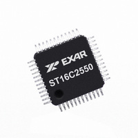
ST16C2550IQ48-F Exar Corporation, ST16C2550IQ48-F Datasheet - Page 9

ST16C2550IQ48-F
Manufacturer Part Number
ST16C2550IQ48-F
Description
IC DUART FIFO 16B 48TQFP
Manufacturer
Exar Corporation
Type
RS- 232 or RS- 485r
Datasheet
1.ST16C2550CJ44-F.pdf
(37 pages)
Specifications of ST16C2550IQ48-F
Number Of Channels
2, DUART
Package / Case
48-TQFP
Features
*
Fifo's
16 Byte
Protocol
RS232, RS485
Voltage - Supply
2.97 V ~ 5.5 V
With False Start Bit Detection
Yes
With Modem Control
Yes
With Cmos
Yes
Mounting Type
Surface Mount
Data Rate
4 Mbps
Supply Voltage (max)
5.5 V
Supply Voltage (min)
2.97 V
Supply Current
3 mA
Maximum Operating Temperature
+ 85 C
Minimum Operating Temperature
- 40 C
Mounting Style
SMD/SMT
Operating Supply Voltage
3.3 V or 5 V
No. Of Channels
2
Supply Voltage Range
2.97V To 5.5V
Operating Temperature Range
-40°C To +85°C
Digital Ic Case Style
TQFP
No. Of Pins
48
Filter Terminals
SMD
Rohs Compliant
Yes
Lead Free Status / RoHS Status
Lead free / RoHS Compliant
Lead Free Status / RoHS Status
Lead free / RoHS Compliant, Lead free / RoHS Compliant
Other names
1016-1256
Available stocks
Company
Part Number
Manufacturer
Quantity
Price
Company:
Part Number:
ST16C2550IQ48-F
Manufacturer:
EXAR21
Quantity:
216
Company:
Part Number:
ST16C2550IQ48-F
Manufacturer:
Exar Corporation
Quantity:
10 000
Part Number:
ST16C2550IQ48-F
Manufacturer:
ST
Quantity:
20 000
REV. 4.4.1
Each UART channel in the C2550 has a standard register set for controlling, monitoring and data loading and
unloading. The configuration register set is compatible to those already available in the standard single
16C550. These registers function as data holding registers (THR/RHR), interrupt status and control registers
(ISR/IER), a FIFO control register (FCR), receive line status and control registers (LSR/LCR), modem status
and control registers (MSR/MCR), programmable data rate (clock) divisor registers (DLL/DLM), and a user
accessible scratch pad register (SPR).
The device does not support direct memory access. The DMA Mode (a legacy term) in this document does not
mean “direct memory access” but refers to data block transfer operation. The DMA mode affects the state of
the RXRDY# A/B and TXRDY# A/B output pins. The transmit and receive FIFO trigger levels provide additional
flexibility to the user for block mode operation. The LSR bits 5-6 provide an indication when the transmitter is
empty or has an empty location(s) for more data. The user can optionally operate the transmit and receive
FIFO in the DMA mode (FCR bit-3=1). When the transmit and receive FIFO are enabled and the DMA mode is
disabled (FCR bit-3 = 0), the C2550 is placed in single-character mode for data transmit or receive operation.
When DMA mode is enabled (FCR bit-3 = 1), the user takes advantage of block mode operation by loading or
unloading the FIFO in a block sequence determined by the programmed trigger level. The following table show
their behavior. Also see Figures
The INTA and INTB interrupt output changes according to the operating mode and enhanced features setup.
Tables 3and 4summarize the operating behavior for the transmitter and receiver. Also see Figures
through 22.
2.4
2.5
2.6
RXRDY# A/B
TXRDY# A/B
INTA/B Pin
INTA/B Pin
P
INS
Channel A and B Internal Registers
DMA Mode
INTA and INTB Outputs
0 = 1 byte.
1 = no data.
0 = THR empty.
1 = byte in THR.
0 = no data
1 = 1 byte
(FIFO D
0 = a byte in THR
1 = THR empty
FCR
T
ABLE
T
BIT
(FIFO D
(FIFO D
ISABLED
ABLE
FCR B
T
FCR B
2: TXRDY#
-0=0
ABLE
3: INTA
17
)
IT
ISABLED
IT
ISABLED
4: INTA
-0 = 0
-0 = 0
through 22.
0 = at least 1 byte in FIFO
1 = FIFO empty.
0 = FIFO empty.
1 = at least 1 byte in FIFO.
AND
AND
(DMA Mode Disabled)
)
)
AND
FCR Bit-3 = 0
INTB P
RXRDY# O
INTB P
0 = at least 1 byte in FIFO
1 = FIFO empty
0 = FIFO below trigger level
1 = FIFO above trigger level
INS
IN
9
O
UTPUTS IN
O
PERATION FOR
PERATION
FCR B
2.97V TO 5.5V DUART WITH 16-BYTE FIFO
1 to 0 transition when FIFO reaches the trigger
level, or time-out occurs.
0 to 1 transition when FIFO empties.
0 = FIFO has at least 1 empty location.
1 = FIFO is full.
IT
FIFO
-0=1 (FIFO E
F
OR
T
(FIFO E
(FIFO E
AND
FCR B
FCR B
RANSMITTER
R
ECEIVER
DMA M
(DMA Mode Enabled)
IT
NABLED
IT
NABLED
NABLED
-0 = 1
-0 = 1
FCR Bit-3 = 1
ODE
)
)
)
ST16C2550
17


