EVAL-ADF7020DB1 Analog Devices Inc, EVAL-ADF7020DB1 Datasheet - Page 3
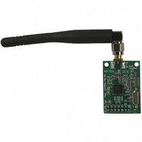
EVAL-ADF7020DB1
Manufacturer Part Number
EVAL-ADF7020DB1
Description
BOARD EVAL ADF7020 902-928MHZ
Manufacturer
Analog Devices Inc
Datasheet
1.EVAL-ADF7020DB2.pdf
(19 pages)
Specifications of EVAL-ADF7020DB1
Module/board Type
Evaluation Board
For Use With/related Products
ADF7020 928MHz
Lead Free Status / RoHS Status
Contains lead / RoHS non-compliant


Preliminary Technical Data
Output Matching Circuit
The ADF7020/ADF7020-1 exhibits optimum performance in
terms of sensitivity, transmit power, and current consumption,
only if its RF input and output ports are properly matched to
the antenna impedance. For cost-sensitive applications, the
ADF7020/ADF7020-1 is equipped with an internal Rx/Tx
switch, which facilitates the use of a simple combined passive
PA/LNA matching network as outlined in Figure 6. Please refer
to Datasheet for more details.
For ease of design the matching and harmonic filter
components are provided for the most commonly used bands
(see Table5-8) Please refer to Application Note AN-764 and
Application Note AN-859 for more details on PA/LNA
matching for the ADF7020 and ADF7020-1 devices.
Antenna
CHOICE OF VCO INDUCTOR FOR ADF7020-1
The ADF7020-1 uses the same VCO core as the ADF7020 but
with the VCO tank inductor (L3) external to allow the user to
set the operating frequency. The frequency of oscillation can be
Harmonic
Filter
Figure 5.. LNA/PA Output Matching Circuit
C3
C2
C1
L2
Vbat
Zopt_pa
L1
Zin_rfin
Zin_rfin
PA_OUT
RFINB
ADF7020
RFIN
+
-
LNA
PA
Rev. Pr C | Page 3 of 19
approximated using the following formula:
The length of the PCB track to the external inductor pad will
effect the total L
external inductor value as measured on the EVAL-ADF7020-
1DBX boards is shown in Figure7. If you are using a different
length of PCB track to the ADI Evaluation boards you need to
take this into consideration. ADIsimPLL will give you the total
external inductance (chip inductor + PCB track) needed for a
given frequency range so that your desired frequency band lies
in the middle of the range where possible. It is also possible to
shift the frequency by use of the VCO Adjust bits which has the
effect of adjusting C
F
590
570
550
530
510
490
470
450
430
410
390
370
350
330
310
290
270
250
230
210
190
170
VCO
0
Figure 6. Direct Output Frequency vs. External Inductor Value(L3)
1
=
2
2
3
ADF7020-1 output frequency vs. external inductor value
π
4
5
(
EXT
L
6
INT
: The ADF7020-1 VCO Frequency range vs.
7
VAR.
8
+
9 10 11 12 13 14 15 16 17 18 19 20 21 22 23 24 25
L
EXT
1
) (
×
EVAL-ADF7020DBX
C
VAR
+
C
FIXED
)
Related parts for EVAL-ADF7020DB1
Image
Part Number
Description
Manufacturer
Datasheet
Request
R


Part Number:
Description:
BOARD EVAL FOR SI270X-A
Manufacturer:
Silicon Laboratories Inc
Datasheet:

Part Number:
Description:
BUCK CONV REF DESIGN KIT IP1201
Manufacturer:
International Rectifier
Datasheet:
Part Number:
Description:
BOARD DEMO SYNC DUAL BUCK CNVTER
Manufacturer:
International Rectifier
Datasheet:
Part Number:
Description:
BOARD DEMO SYNC BUCK CONVETER
Manufacturer:
International Rectifier
Datasheet:

Part Number:
Description:
EVALBOARD/EB Omnidirectional microphone - Analog
Manufacturer:
Analog Devices
Datasheet:
Part Number:
Description:
EVALBOARD/EB Omnidirectional microphone - Analog
Manufacturer:
Analog Devices
Datasheet:


Part Number:
Description:
BOARD EVAL LED DRIVER LT3756
Manufacturer:
Linear Technology
Datasheet:

Part Number:
Description:
BOARD EVAL FOR AD7741/7742
Manufacturer:
Analog Devices Inc
Datasheet:

Part Number:
Description:
±1.7g Dual-Axis IMEMS Accelerometer Evaluation Board
Manufacturer:
Analog Devices Inc
Datasheet:

Part Number:
Description:
IC MULTIPLIER ANALOG 8-SOIC T/R
Manufacturer:
Analog Devices Inc
Datasheet:

Part Number:
Description:
IC ANALOG MULTIPLIER 8-DIP
Manufacturer:
Analog Devices Inc
Datasheet:
Part Number:
Description:
IC ANALOG MULTIPLIER 8-SOIC
Manufacturer:
Analog Devices Inc
Datasheet:
Part Number:
Description:
IC ANALOG MULTIPLIER 8-DIP
Manufacturer:
Analog Devices Inc
Datasheet: