EVAL-ADF7020DB1 Analog Devices Inc, EVAL-ADF7020DB1 Datasheet - Page 8
EVAL-ADF7020DB1
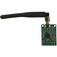
Manufacturer Part Number
EVAL-ADF7020DB1
Description
BOARD EVAL ADF7020 902-928MHZ
Manufacturer
Analog Devices Inc
Datasheet
1.EVAL-ADF7020DB2.pdf
(19 pages)
Specifications of EVAL-ADF7020DB1
Module/board Type
Evaluation Board
For Use With/related Products
ADF7020 928MHz
Lead Free Status / RoHS Status
Contains lead / RoHS non-compliant


EVAL-ADF7020-XDBX
GETTING STARTED WITH THE ADF7020 AND ADF7020-1
The evaluation performed will be specific to each application,
but this section will enable users to familiarise themselves with
the features of the ADF7020/ADF7020-1.
Initial Setup
As described in the Hardware Description section, the
evaluation board is divided into two; an RF module containing
the ADF7020 and a mother-board which accepts the RF
module and contains the power supply block and some I/O
pins. You need to mount the RF module onto the mother-
board, ensuring correct alignment by having the drill-holes in
the module above the screw-holders on the mother board.
Apply 3V to the VDD pin, with the regulator jump switch K3
connected to position B. An ammeter can be placed in series
with the supply by connecting to Iin and Iout, otherwise place a
wire short across Iin and Iout. The ChipEnable link (K1) is
initially connected to GND, so you should connect this to VDD
for normal operation. Once CE is High, the part will become
active and approximately 2.2mA is drawn. The default
conditions on power-up are:
Crystal Oscillator circuit
CLKout
PLL
PA
Regulators
Muxout
To check the part has powered-up correctly, monitor the
XCLKOUT pin (pin4 on mother-board test-header), this should
be a 3Vp-p square wave with a frequency of XTAL_frequency/8.
Also the voltage on the Regulator pins should be between 2.0V
and 2.2V, you can check this by probing the top of C5 (VREG4
pin) on the RF module.
Evaluating the ADF7020 in Rx and Tx modes
Before setting up an RF link, it is usually informative to
evaluate the ADF7020/ADF7020-1 in either Tx mode or Rx
mode. The typical setup for this is shown in Figures 12 and 13.
To select between Tx and Rx modes in the software select the
required mode in the top left of the front display panel.
Note: All of the ADF7020 and ADF7021 daughter boards have
an 11.0592MHz xtal except for the ADF7020-1DB7 which has a
9.8304MHz xtal. In the following text for simplicity it will be
assumed that the crystal is 11.0592MHz.
Test Procedure for the ADF7020 in Tx Mode
Use a supply of 3V and the setup as shown in Figure 12. At first
you can just connect RxTxData to GND.
1.
Ensure that the CE Link is connected to High. The current
drawn should be typically 2.2mA. The regulators are now
powered-up.
ON
ON (div-by-8)
OFF
OFF
ON
Regulator Ready
Rev. Pr C | Page 8 of 19
2.
3.
Check XCLKOUT (Pin4 on test-header) using a scope.
Signal should be 3Vp-p square wave with frequency equal
to XTAL_FREQ/8. This is the power-up default. The
crystal is oscillating and the XCLKOUT feature is working
correctly.
Using the ADF7020 or ADF7020-1 Software, setup the
following Tx parameters:
a.
b.
c.
d.
Figure 12. Evaluation board setup for Tx mode
Ensure Tx Mode is selected in Mode sub-window
Click on Synth Settings and set
Click Charge-pump current, set this to 1.44mA
Bias Currents – Click VCO/LNA/Mixer… button
iii. Fcrystal = 11.0592MHz
iv. FPFD = 11.0592MHz
ii. You can also toggle the VCO divide-by-
ii. Set VCO bias to 2.75mA (ADF7020)
v. Hit Calculate and Load Now
i. RF Channel Frequency (Direct Output)
i. VCO Adjust = 0 (See datasheet for
Preliminary Technical Data
to your desired frequency.
2 button to get half this frequency. This
divider is placed outside the PLL loop
and thus does not affect the N-Divider
settings. For example to obtain 433MHz
from the ADF7020, you should set the
Direct Output to 866MHz and enable
divide-by-2.
recommended settings)
For ADF7020-1 set VCO-bias according
to datasheet table 5
Related parts for EVAL-ADF7020DB1
Image
Part Number
Description
Manufacturer
Datasheet
Request
R


Part Number:
Description:
BOARD EVAL FOR SI270X-A
Manufacturer:
Silicon Laboratories Inc
Datasheet:

Part Number:
Description:
BUCK CONV REF DESIGN KIT IP1201
Manufacturer:
International Rectifier
Datasheet:
Part Number:
Description:
BOARD DEMO SYNC DUAL BUCK CNVTER
Manufacturer:
International Rectifier
Datasheet:
Part Number:
Description:
BOARD DEMO SYNC BUCK CONVETER
Manufacturer:
International Rectifier
Datasheet:

Part Number:
Description:
EVALBOARD/EB Omnidirectional microphone - Analog
Manufacturer:
Analog Devices
Datasheet:
Part Number:
Description:
EVALBOARD/EB Omnidirectional microphone - Analog
Manufacturer:
Analog Devices
Datasheet:


Part Number:
Description:
BOARD EVAL LED DRIVER LT3756
Manufacturer:
Linear Technology
Datasheet:

Part Number:
Description:
BOARD EVAL FOR AD7741/7742
Manufacturer:
Analog Devices Inc
Datasheet:

Part Number:
Description:
±1.7g Dual-Axis IMEMS Accelerometer Evaluation Board
Manufacturer:
Analog Devices Inc
Datasheet:

Part Number:
Description:
IC MULTIPLIER ANALOG 8-SOIC T/R
Manufacturer:
Analog Devices Inc
Datasheet:

Part Number:
Description:
IC ANALOG MULTIPLIER 8-DIP
Manufacturer:
Analog Devices Inc
Datasheet:
Part Number:
Description:
IC ANALOG MULTIPLIER 8-SOIC
Manufacturer:
Analog Devices Inc
Datasheet:
Part Number:
Description:
IC ANALOG MULTIPLIER 8-DIP
Manufacturer:
Analog Devices Inc
Datasheet: