MGA-634P8-BLKG Avago Technologies US Inc., MGA-634P8-BLKG Datasheet
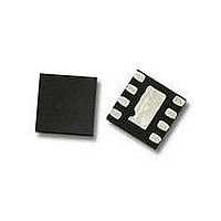
IC LNA ULTRA LOW NOISE ACT BIAS

MGA-634P8-BLKG

Manufacturer Part Number
MGA-634P8-BLKG
Description
IC LNA ULTRA LOW NOISE ACT BIAS
Manufacturer
Avago Technologies US Inc.
Type
High Linearity Low Noise Amplifierr
Datasheets

Specifications of MGA-634P8-BLKG

Package / Case
8-WFDFN Exposed Pad
Current - Supply
48mA
Frequency
1.5GHz ~ 2.3GHz
Gain
17.4dB
Noise Figure
0.44dB
P1db
21dBm
Rf Type
CDMA, GSM
Test Frequency
1.9GHz
Voltage - Supply
5V
Mounting Style
SMD/SMT
Operating Frequency
1.5 GHz to 2.3 GHz
Operating Supply Voltage
5 V
Supply Current
50 mA
Maximum Operating Temperature
+ 125 C
Minimum Operating Temperature
- 55 C
Manufacturer's Type
Low Noise Amplifier
Number Of Channels
1
Frequency (max)
1.9GHz
Operating Supply Voltage (max)
5.5V
Package Type
QFN EP
Mounting
Surface Mount
Pin Count
8
Operating Temp Range
-40C to 85C
Operating Temperature Classification
Industrial
Lead Free Status / RoHS Status
Lead free / RoHS Compliant
Lead Free Status / RoHS Status
Lead free / RoHS Compliant, Lead free / RoHS Compliant

Available stocks

Company
Part Number
Manufacturer
Quantity
Price
Part Number:
MGA-634P8-BLKG
Manufacturer:
AVAGO
Quantity:
12 000
MGA-634P8
Ultra Low Noise, High Linearity Low Noise Amplifi er
Data Sheet
Description
Avago Technologies’ MGA-634P8 is an economical, easy-
to-use GaAs MMIC Low Noise Amplifi er (LNA). The LNA has
low noise and high linearity achieved through the use of
Avago Technologies’ proprietary 0.25um GaAs Enhance-
ment-mode pHEMT process. It is housed in a miniature 2.0
x 2.0 x 0.75mm
It is designed for optimum use from 1.5 GHz up to 2.3 GHz.
The compact footprint and low profi le coupled with low
noise, high gain and high linearity make the MGA-634P8
an ideal choice as a low noise amplifi er for cellular infra-
structure for GSM and CDMA. For optimum performance at
lower frequency from 450MHz up to 1.5GHz, MGA-633P8
is recommended. For optimum performance at higher
frequency from 2.3GHz up to 4GHz, MGA-635P8 is recom-
mended. All these 3 products, MGA-633P8, MGA-643P8
and MGA-653P8 share the same package and pinout con-
fi guration.
Pin Confi guration and Package Marking
2.0 x 2.0 x 0.75 mm
Pin 1 – Vbias
Pin 2 – RFinput
Pin 3 – Not Used
Pin 4 – Not Used
Note:
Package marking provides orientation and identifi cation
“34” = Device Code, where X is the month code.
[1]
[2]
[3]
[4]
Top View
34X
3
8-pin Quad-Flat-Non-Lead (QFN) package.
[8]
[7]
[6]
[5]
3
8-lead QFN
Attention: Observe precautions for
handling electrostatic sensitive devices.
ESD Machine Model = 70 V (Class A)
ESD Human Body Model = 500 V (Class 1B)
Refer to Avago Application Note A004R:
Electrostatic Discharge, Damage and Control.
Pin 5 – Not Used
Pin 6 – Not Used
Pin 7 – RFoutput/Vdd
Pin 8 – Not Used
Centre tab - Earth
[8]
[7]
[6]
[5]
Bottom View
[1]
[2]
[3]
[4]
Features
 Ultra Low noise Figure
 High linearity performance
 GaAs E-pHEMT Technology
 Low cost small package size: 2.0x2.0x0.75 mm
 Excellent uniformity in product specifi cations
 Tape-and-Reel packaging option available
Specifi cations
1.9 GHz; 5V, 48mA
 17.4 dB Gain
 0.44 dB Noise Figure
 15.5 dB Input Return Loss
 36 dBm Output IP3
 21 dBm Output Power at 1dB gain compression
Applications
 Low noise amplifi er for cellular infrastructure for GSM
 Other ultra low noise application.
Simplifi ed Schematic
Notes:
 The schematic is shown with the assumption that similar PCB is used
 Detail of the components needed for this product is shown in Table 1.
 Enhancement mode technology employs positive gate voltage,
 Good RF practice requires all unused pins to be earthed.
RFin
TDS-CDMA, and CDMA.
for all MGA-633P8, MGA-634P8 and MGA-635P8.
thereby eliminating the need of negative gate voltage associated
with conventional depletion mode devices.
C5
C3
C1
L1
R1
[1]
[2]
[3]
[4]
Rbias
bias
[1]
R2
[8]
[7]
[6]
[5]
Vdd
L2
C2
C6
C4
3
RFout

Related parts for MGA-634P8-BLKG

MGA-634P8-BLKG Summary of contents

Page 1

... It is designed for optimum use from 1.5 GHz up to 2.3 GHz. The compact footprint and low profi le coupled with low noise, high gain and high linearity make the MGA-634P8 an ideal choice as a low noise amplifi er for cellular infra- structure for GSM and CDMA. For optimum performance at lower frequency from 450MHz ...

Page 2

Absolute Maximum Rating T =25°C A Symbol Parameter Device Voltage output to ground V Gate Voltage bias Input Power in,max (V = 5.0V mA [2] P Total Power ...

Page 3

Product Consistency Distribution Charts LSL Figure 1. Idd @ 1.9GHz, 5V, 48mA Mean = 48 LSL OIP3 Min: 33 Mean Figure ...

Page 4

Demo Board Layout Figure 5. Demo Board Layout Diagram – Recommended PCB material is 10 mils Rogers RO4350. – Suggested component values may vary according to layout and PCB material. Table 1. Component list for 1.9 GHz matching Part Size ...

Page 5

... MGA-634P8 Typical Performance RF performance 25°C, Vdd = 5V 50mA, measured using 50ohm input and output board, unless otherwise A stated. OIP3 test condition 1.9 GHz, F RF1 0.44 0.42 0.4 0.38 0.36 0.34 0.32 0 Idd (mA) Figure 7. Fmin vs Idd 1.9GHz Idd(mA) Figure 9. Gain vs Idd at 5V Tuned for Optimum OIP3 and Fmin at 1.9GHz. ...

Page 6

Idd (mA) Figure 13. OP1dB vs Idd at 5V Tuned for Optimum OIP3 and Fmin at 1.9GHz 0.8 0.7 0.6 0.5 0.4 0.3 0.2 ...

Page 7

... Frequency (GHz) Figure 19. OP1dB vs Frequency and Temperature for Optimum OIP3 and Fmin at 5V 50mA Below is the table showing the MGA-634P8 Refl ection Coeffi cient Parameters tuned for maximum OIP3, Vdd = 5V, Idd = 50mA Gamma Load position Frequency (GHz) Magnitude 1.5 ...

Page 8

... MGA-634P8 Typical Performance in Demoboard RF performance 25°C, Vdd = 5V, Rbias = 5.6 kOhm, measured on demo board in Figure. 5 with component list in A Table 1 for 1.9 GHz matching, unless or otherwise stated. 1 0.9 0.8 0.7 0.6 0.5 0.4 0.3 0.2 0.1 0 1.5 1.7 1.9 2.1 2.3 Frequency (GHz) Figure 21 ...

Page 9

Rbias (KΩ) Figure 27. Idd vs Rbias 1 0.9 0.8 0.7 0.6 0.5 0.4 0.3 0.2 0.1 0 1.5 1.7 1.9 2.1 2.3 Frequency (GHz) Figure 29. NF ...

Page 10

... MGA-634P8 Typical Scattering Parameters, Vdd = 5V, Idd = 50mA S11 Freq GHz Mag. Ang. 0.10 0.23 -163.34 0.50 0.48 136.70 0.90 0.37 37.53 1.00 0.27 9.09 1.50 0.09 -176.43 1.90 0.15 115.81 2.00 0.16 104.04 2.50 0.21 62.05 3.00 0.24 24.06 4.00 0.28 -49 ...

Page 11

... Top View 0.60±0.050 Exp. DAP 0.35±0.050 0.25±0.050 Bottom View 11 Part Number Ordering Information  Part Number Ang. R   opt n/50 MGA-634P8-BLKG 68.4 0.0484 MGA-634P8-TR1G 113.6 0.0442 120.4 0.0526 131.1 0.0444 151.5 0.0476 0.203 Ref. 0.000–0.05 0.75±0.05 ...

Page 12

Recommended PCB Land Pattern and Stencil Design 2.20 1.75 0.00 0.80 0.50 0.25 0.45 0.30 R0.15 Land Pattern Combination of Land Pattern and Stencil Opening Note: 1. Recommended Land Pattern and Stencil Opening 2. Stencil thickness is 0.1mm (4 mils) ...

Page 13

Device Orientation REEL USER FEED DIRECTION COVER TAPE Tape Dimensions 10° MAX A O DESCRIPTION CAVITY LENGTH WIDTH DEPTH PITCH BOTTOM HOLE DIAMETER PERFORATION DIAMETER PITCH POSITION CARRIER TAPE WIDTH THICKNESS COVER TAPE WIDTH TAPE ...

Page 14

Reel Dimensions – 7 inch 6.25mm EMBOSSED LETTERS LETTERING THICKNESS: 1.6mm SEE DETAIL "X" SLOT HOLE "b" SLOT HOLE(2x) 180° APART FRONT VIEW RECYCLE LOGO R10.65 R5.2 SLOT HOLE ‘b’ EMBOSSED RIBS RAISED: 0.25mm, WIDTH: 1.25mm ...

Related keywords