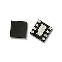
MGA-634P8-BLKG Avago Technologies US Inc., MGA-634P8-BLKG Datasheet - Page 2

MGA-634P8-BLKG
Manufacturer Part Number
MGA-634P8-BLKG
Description
IC LNA ULTRA LOW NOISE ACT BIAS
Manufacturer
Avago Technologies US Inc.
Type
High Linearity Low Noise Amplifierr
Specifications of MGA-634P8-BLKG
Package / Case
8-WFDFN Exposed Pad
Current - Supply
48mA
Frequency
1.5GHz ~ 2.3GHz
Gain
17.4dB
Noise Figure
0.44dB
P1db
21dBm
Rf Type
CDMA, GSM
Test Frequency
1.9GHz
Voltage - Supply
5V
Mounting Style
SMD/SMT
Operating Frequency
1.5 GHz to 2.3 GHz
Operating Supply Voltage
5 V
Supply Current
50 mA
Maximum Operating Temperature
+ 125 C
Minimum Operating Temperature
- 55 C
Manufacturer's Type
Low Noise Amplifier
Number Of Channels
1
Frequency (max)
1.9GHz
Operating Supply Voltage (max)
5.5V
Package Type
QFN EP
Mounting
Surface Mount
Pin Count
8
Operating Temp Range
-40C to 85C
Operating Temperature Classification
Industrial
Lead Free Status / RoHS Status
Lead free / RoHS Compliant
Lead Free Status / RoHS Status
Lead free / RoHS Compliant, Lead free / RoHS Compliant
Available stocks
Company
Part Number
Manufacturer
Quantity
Price
Company:
Part Number:
MGA-634P8-BLKG
Manufacturer:
AVAGO
Quantity:
12 000
Absolute Maximum Rating
Electrical Specifi cations
RF performance at T
listed in Table 1 for 1.9 GHz matching.
Notes:
1. Measurements at 1.9 GHz obtained using demo board described in Figure 1.
2. OIP3 test condition: F
3. For NF data, board losses of the input have not been de-embedded.
4. Use proper bias, heatsink and derating to ensure maximum device temperature is not exceeded. See absolute maximum ratings and application
2
Symbol
V
V
P
P
T
T
T
Symbol
I
Gain
OIP3
NF
OP1dB
IRL
ORL
REV ISOL
dd
stg
amb
diss
j
dd
bias
in,max
note for more details.
[3]
[2]
Parameter
Device Voltage,
RF output to ground
Gate Voltage
CW RF Input Power
(V
Total Power Dissipation
Junction Temperature
Storage Temperature
Ambient Temperature
dd
Parameter and Test Condition
Drain Current
Gain
Output Third Order Intercept Point
Output Power at 1dB Gain Compression
Input Return Loss, 50 source
Output Return Loss, 50 load
Reverse Isolation
Noise Figure
= 5.0V, I
A
RF1
= 25°C, V
= 1.9 GHz, F
d
[1], [4]
[1]
= 50 mA)
T
A
=25°C
dd
RF2
= 5V, R
[2]
= 1.901 GHz with input power of -10dBm per tone.
bias
= 5.6 kOhm, 1.9 GHz, measured on demo board in Figure 1 with component
Units
V
V
dBm
W
°C
°C
°C
Absolute Maximum
5.5
0.7
+20
0.5
150
-65 to 150
-40 to 85
Units
mA
dB
dBm
dB
dBm
dB
dB
dB
Thermal Resistance
Notes:
1. Operation of this device in excess of any of
2. Power dissipation with device turned on.
3. Thermal resistance measured using Infra-Red
Thermal Resistance
(V
jc
dd
these limits may cause permanent damage.
Board temperature T
16mW/°C for T
Measurement Technique
= 62°C/W
= 5.0V, I
Min.
37
16.1
33
dd
= 50mA)
B
>119°C.
Typ.
48
17.4
36
0.44
21
15.5
13
30
[3]
B
is 25°C. Derate at
Max.
61
19.1
0.69


