AMMP-6130-TR1G Avago Technologies US Inc., AMMP-6130-TR1G Datasheet - Page 2
AMMP-6130-TR1G
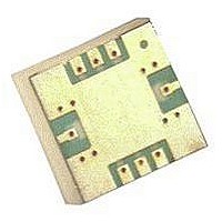
Manufacturer Part Number
AMMP-6130-TR1G
Description
IC MMIC PWR AMP 30GHZ 8SMD
Manufacturer
Avago Technologies US Inc.
Type
Power Amplifierr
Datasheet
1.AMMP-6130-TR2G.pdf
(8 pages)
Specifications of AMMP-6130-TR1G
Gain
18.5dB
Current - Supply
200mA
Frequency
15GHz, 30GHz
Package / Case
8-SMD
Rf Type
VSAT, DBS
Voltage - Supply
3.5 V ~ 5 V
Supply Current
200mA
Supply Voltage Range
3.5V To 5V
Rf Ic Case Style
SMD
No. Of Pins
8
Frequency Max
30GHz
Termination Type
SMD
Frequency Min
1GHz
Supply Voltage Max
5V
Number Of Channels
1
Power Supply Requirement
Single
Single Supply Voltage (min)
3.5V
Single Supply Voltage (typ)
4.5V
Single Supply Voltage (max)
5V
Package Type
SMT
Dual Supply Voltage (min)
Not RequiredV
Dual Supply Voltage (typ)
Not RequiredV
Dual Supply Voltage (max)
Not RequiredV
Pin Count
8
Mounting
Surface Mount
Filter Terminals
SMD
Rohs Compliant
Yes
Lead Free Status / RoHS Status
Lead free / RoHS Compliant
Noise Figure
-
P1db
-
Test Frequency
-
Lead Free Status / Rohs Status
Compliant


Absolute Maximum Ratings
Notes.
1. Operation in excess of any of these conditions may result in perma-
AMMP-6130 RF Specifications
TA= 25°C, Vdd = 4.5 V, Idd = 200mA, Zo=50 Ω, Pin=5dBm
Notes.
4. Small/Large -signal data measured in a fully de-embedded test fixture form TA = 25°C.
5. All tested parameters guaranteed with measurement accuracy +/-1dB/dBm/dBc.
Typical Distribution of Conversion Gain and Output Power based on 1000 parts
Conversion Gain at 30GHz
Symbol
Freq
Gain
Pout
FS
3H Sup
Sym
Vdd
Idd
Pin
Tch
Tstg
Tmax
nent damage to this device. The absolute maximum ratings for Vdd,
Idd and Pin were determined at an ambient temperature of 25°C
unless noted otherwise.
Parameters/Condition
Drain to Ground Voltage
Drain Current
RF CW Input Power Max
Max channel temperature
Storage temperature
Maximum Assembly Temp
Parameters and Test Conditions
Operational Frequency
Conversion Gain
Output Power
Fundamental Suppression
3rd Harmonic Suppression
StDev = 0.46
(5)
(1)
(4,5)
(4,5)
Unit
V
mA
dBm
C
C
C
Max
5
300
15
+150
-65 +150
260 for 20s
Frequency
30
30
30
DC Specifications/ Physical Properties
2. Ambient operational temperature TA=25°C unless noted
3. Channel-to-backside Thermal Resistance (Tchannel = 34°C) as mea-
Output Power at 30GHz
Sym
Idd
Vd
qjc
sured using infrared microscopy. Thermal Resistance at backside
temp. (Tb) = 25°C calculated from measured data.
Units
GHz
dB
dBm
dBc
dBc
Parameter and Test
Condition
Drain Supply Current
under any RF power
drive and temp.(V
V)
Drain Supply Voltage
Thermal Resistance
Minimum
14
19
d
StDev = 0.39
=4.5
(3)
Maximum
18.5
23.5
Unit
mA
V
C/W
(2)
Min
3.5
Typ
200
4.5
45
Typical
30
16
21
60
50
Max
250
5
Related parts for AMMP-6130-TR1G
Image
Part Number
Description
Manufacturer
Datasheet
Request
R

Part Number:
Description:
IC MMIC PWR AMP 30GHZ 8SMD
Manufacturer:
Avago Technologies US Inc.
Datasheet:

Part Number:
Description:
30 GHz Doubler W/Amp - Pkg
Manufacturer:
Avago Technologies US Inc.
Datasheet:

Part Number:
Description:
IC AMP GP HI PWR 6-20GHZ 8-SMD
Manufacturer:
Avago Technologies US Inc.
Datasheet:

Part Number:
Description:
IC AMP GP HI PWR 6-20GHZ 8-SMD
Manufacturer:
Avago Technologies US Inc.
Datasheet:

Part Number:
Description:
IC MMIC AMP HGA 6-20GHZ 8SMD
Manufacturer:
Avago Technologies US Inc.
Datasheet:

Part Number:
Description:
IC MMIC AMP HGA 6-20GHZ 8SMD
Manufacturer:
Avago Technologies US Inc.
Datasheet:
Part Number:
Description:
IC MMIC LOW NOISE 6-20GHZ 8-SMD
Manufacturer:
Avago Technologies US Inc.
Datasheet:
Part Number:
Description:
IC AMP GP HI PWR 6-20GHZ 8-SMD
Manufacturer:
Avago Technologies US Inc.
Datasheet:

Part Number:
Description:
6-20 GHz High Gain Amp In SMT Pkg
Manufacturer:
Avago Technologies US Inc.
Datasheet:

Part Number:
Description:
Power Amp, MMIC, 6-18GHz Pkg
Manufacturer:
Avago Technologies US Inc.
Datasheet:

Part Number:
Description:
OPTOCOUPLER GATE DRV 2A 16-SOIC
Manufacturer:
Avago Technologies US Inc.
Datasheet:
Part Number:
Description:
OPTOCOUPLER 2CH 2.5A 16-SOIC
Manufacturer:
Avago Technologies US Inc.
Datasheet:

Part Number:
Description:
OPTOCOUPLER GATE DRV 0.4A 16SOIC
Manufacturer:
Avago Technologies US Inc.
Datasheet:

Part Number:
Description:
OPTOCOUPLER 2.0A 250KHZ 8-DIP
Manufacturer:
Avago Technologies US Inc.
Datasheet:

Part Number:
Description:
OPTOCOUPLER 2.0A 250KHZ GW 8-SMD
Manufacturer:
Avago Technologies US Inc.
Datasheet: